Introduction
In modern automotive and industrial electronic systems, DC-DC converters have become increasingly important due to the rising demand for high efficiency and reliable operation across a wide load and environmental conditions. Traditional analog-controlled converters often struggle to balance fast transient response, stability, and digital integration requirements in advanced CMOS processes. These challenges motivate the design of a digitally assisted power converter that can achieve both high performance and high robustness.
This project aims to design a digital PID-controlled CMOS DC-DC buck converter featuring zero-crossing detection (ZCD) for enhanced switching efficiency (in DCM) using the TSMC 65nm process. The objective is to achieve stable regulation across a wide output range while minimizing switching loss and conduction loss, and improving transient response. By leveraging a digital PID controller, the converter benefits from programmability, PVT tolerance, and predictable loop dynamics compared with traditional analog control methods.
The PWM voltage mode control is used for the proposed converter. The input voltage is 2.5V, and the output voltage can be regulated to 0.9~2.0V. The maximum load current is 500mA, with 20~50mV expected voltage ripple and 100mA current ripple. The detailed specifications are listed in the "Specifications" section.
System Architecture
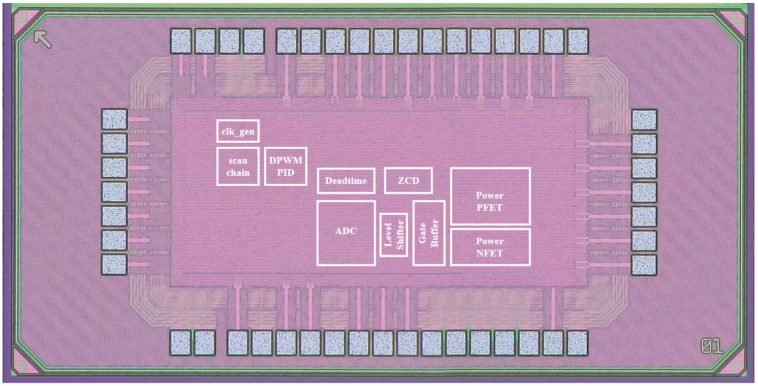
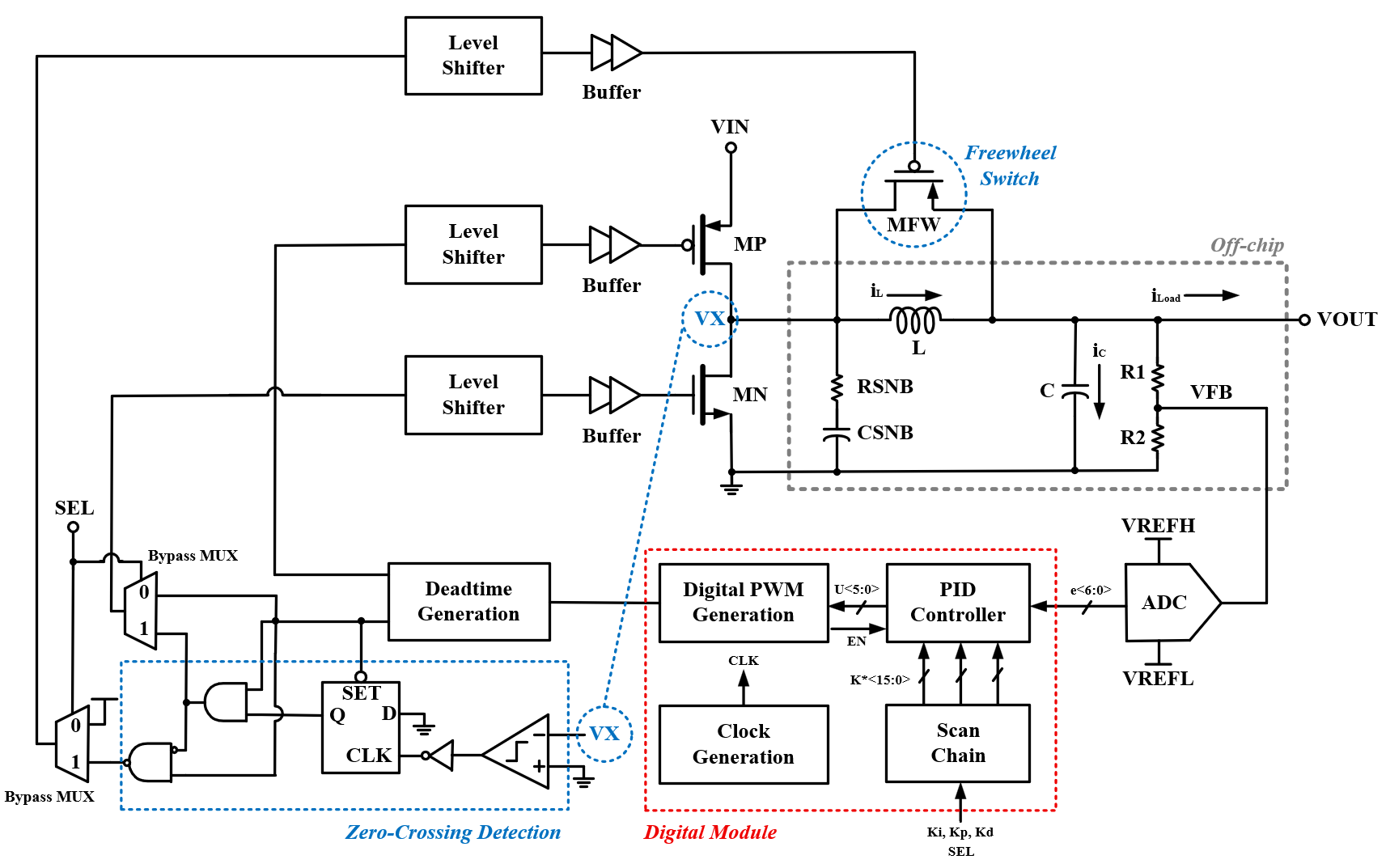
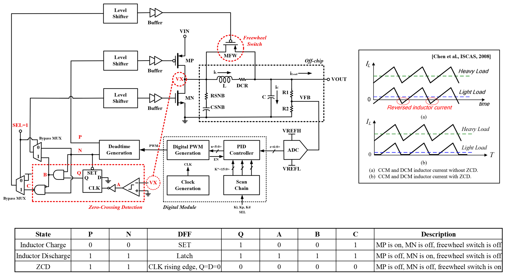
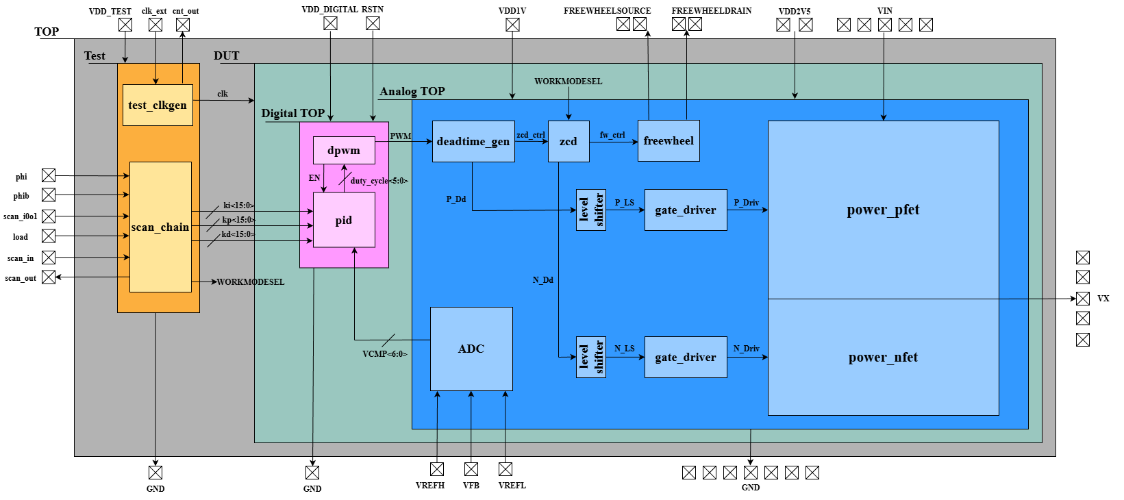
Blocks designed in the proposed converter include flash ADC, power stage, gate drivers, non-overlap dead-time generation, DCVS level shifters, a PID controller, a digital PWM waveform generation, a zero-crossing detection (ZCD) module, a scan chain, and a clock generation. The LCR output power stage is implemented off-chip due to its large passive component requirements.
Main Components
Power Stage
The power stage consists of the high-side and low-side switches (implemented using TSMC 65 nm 2.5V I/O devices) and an off-chip LC filter. The values of the inductor and output capacitor are determined based on charge-conservation principles and the slope calculations of the inductor current waveform. All necessary parameters are selected to ensure they are compatible with and can be directly applied to the design formulas.
The lengths of the switches are typically set to the minimum allowable value to minimize their turn-on resistance for a given width. The width sizing is determined by balancing conduction loss and switching loss: conduction loss decreases with increasing width, whereas switching loss increases with width. Therefore, for a given load current, there exists an optimal device width at which these two losses are equal if no other loss mechanisms are considered.
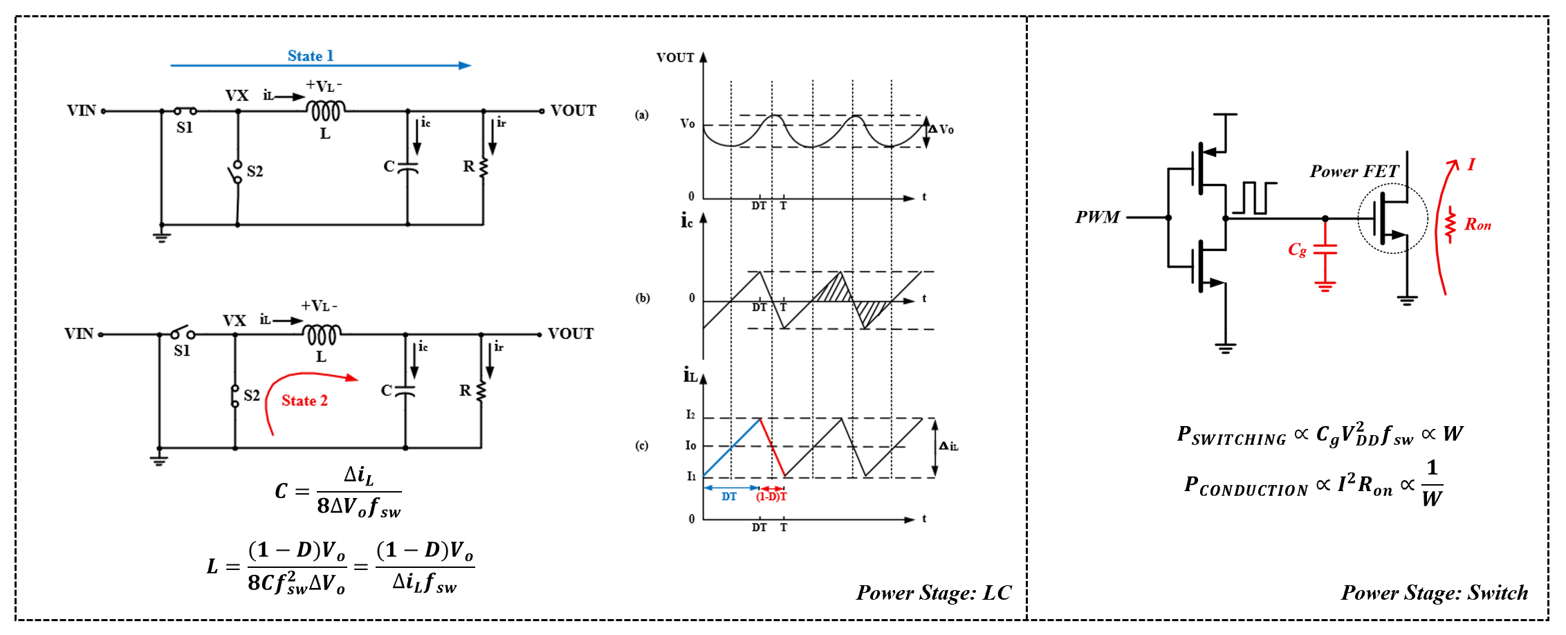
In practice, additional factors must be included, such as the power consumption of other circuit blocks and the inductor’s DCR. The former is often negligible, while the latter must be accounted for by identifying practical inductors on Digi-Key, checking their DCR specifications, and incorporating those values into simulation.
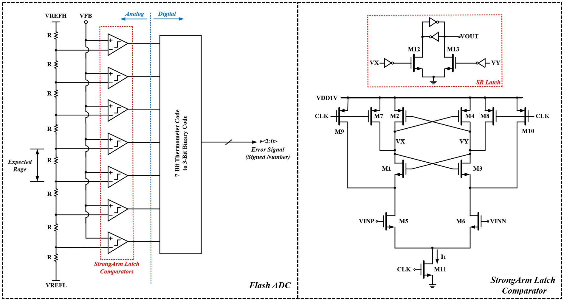
Flash ADC and Comparator
The converter employs a flash ADC architecture to provide the high-speed conversion needed for fast control loops. Because a buck converter does not require high resolution, a 3-bit ADC was selected to balance performance, area, and complexity, resulting in a reasonable number of comparators. Each comparator uses a strong-arm latch topology, chosen for its high speed and low power consumption.
To further reduce the comparators' delay and input-referred offset, the input differential pair is upsized to improve transconductance and mitigate device mismatch. The remaining transistors in the latch are kept smaller than the input-pair to minimize parasitic capacitances, thereby lowering delay. Additionally, decoupling capacitors can be introduced to reduce clock feedthrough and kickback noise, improving overall comparator accuracy.
Dead-Time Generation
To reduce the additional power consumption caused by shoot-through current during switching, a dead-time generation circuit is implemented to produce two non-overlapping PWM waveforms. During the designated dead time, the gate of the power PMOSFET is held high while the gate of the power NMOSFET is kept low, ensuring that both devices cannot turn on simultaneously and eliminating shoot-through current.
However, this introduces a design trade-off. When the dead time is too long, the body diode of one device may conduct, causing a voltage drop and leading to extra power loss and potential device stress. For instance, if the NMOSFET body diode becomes forward-biased, the PMOSFET can experience a VDS that exceeds its nominal voltage. Prolonged or excessive dead time may therefore cause junction breakdown even when the PMOSFET is off. A commonly used guideline is to set the dead time to approximately 1% of the PWM period.
Level Shifter
Because the core operates at 1V, the generated PWM signal is also within the 0–1V domain and therefore cannot directly drive the 2.5V I/O devices used in the power stage. To address this, a 1V-to-2.5V level shifter based on the differential cascode voltage switch (DCVS) topology is implemented.
To reduce shoot-through current during transitions, the pull-down transistors (M1 and M2) are sized much larger than the pull-up transistors (M3 and M4). For example, when VIN transitions from low to high, VOUTN is pulled down to ground, turning on M4, which in turn pulls VOUT up to VDD2V5 while M3 turns off. During this transition, there can be a short interval in which both M1 and M3 are simultaneously on—specifically when VIN > Vth1 and VOUT < (VDD2V5 − |Vth3|). By making the pull-down devices stronger than the pull-up devices, the middle node is discharged more quickly, reducing the duration of this short-circuit condition and thereby lowering shoot-through current.
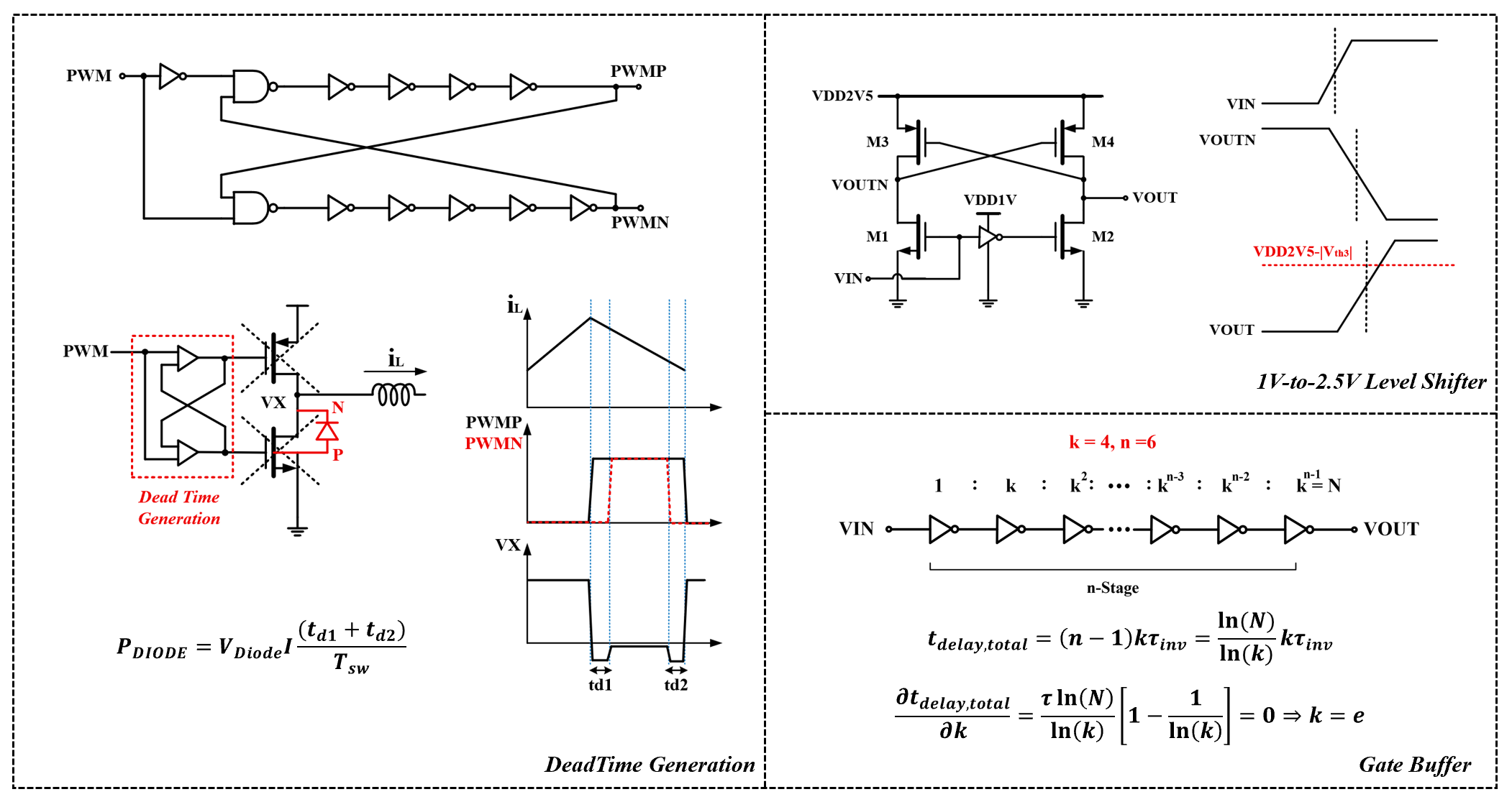
Gate Buffer
To drive the large MOSFET switches in the power stage, an inverter-chain gate buffer is employed to minimize overall propagation delay. The optimal sizing ratio k and the number of stages n are obtained by minimizing the total path delay (i.e., setting the derivative of the delay expression to zero). Although the theoretical optimum for the stage ratio is e, a larger even value k=4 is used in practice to account for non-idealities beyond gate capacitance and ensure better matching.
Zero-Crossing Detection
When the converter operates in DCM, the inductor current can reverse direction, which degrades efficiency. To mitigate this issue, a zero-crossing detection (ZCD) module is added. By sensing the switching node VX through a comparator, the ZCD logic determines whether the NMOS switch should be turned off. In addition, a freewheel switch is added to short the inductor and dissipate the residual energy stored in it.
PID Controller
In digitally controlled DC-DC converters, a Proportional–Integral–Derivative (PID) controller is commonly employed to regulate the output voltage. The proportional term provides immediate correction based on the voltage error, the integral term removes steady-state offset by accumulating long-term error, and the derivative term enhances transient response by reacting to rapid changes in the output. In this design, the PID controller operates at 1MHz, as it is triggered by the 64MHz DPWM every 64 clock cycles, resulting in a 1MHz PWM switching frequency. All three PID coefficients are implemented as 16-bit values and are loaded into the controller through the scan chain.
Digital PWM Waveform Generation
A counter-based Digital Pulse Width Modulation (DPWM) module is used to generate the switching signal for the power stage. In this design, the DPWM used a 6-bit up-counter clocked at 64MHz. The duty cycle is determined by comparing the counter value with a 6-bit digital control word provided by the PID controller. When the counter value is lower than the control word, the output remains high; otherwise, it switches low. Because a 6-bit counter provides 64 time slots, the resulting PWM switching frequency is 64MHz/64=1MHz. This architecture offers simple implementation, linear duty-cycle resolution, and robust operation suitable for digitally controlled DC-DC converters.
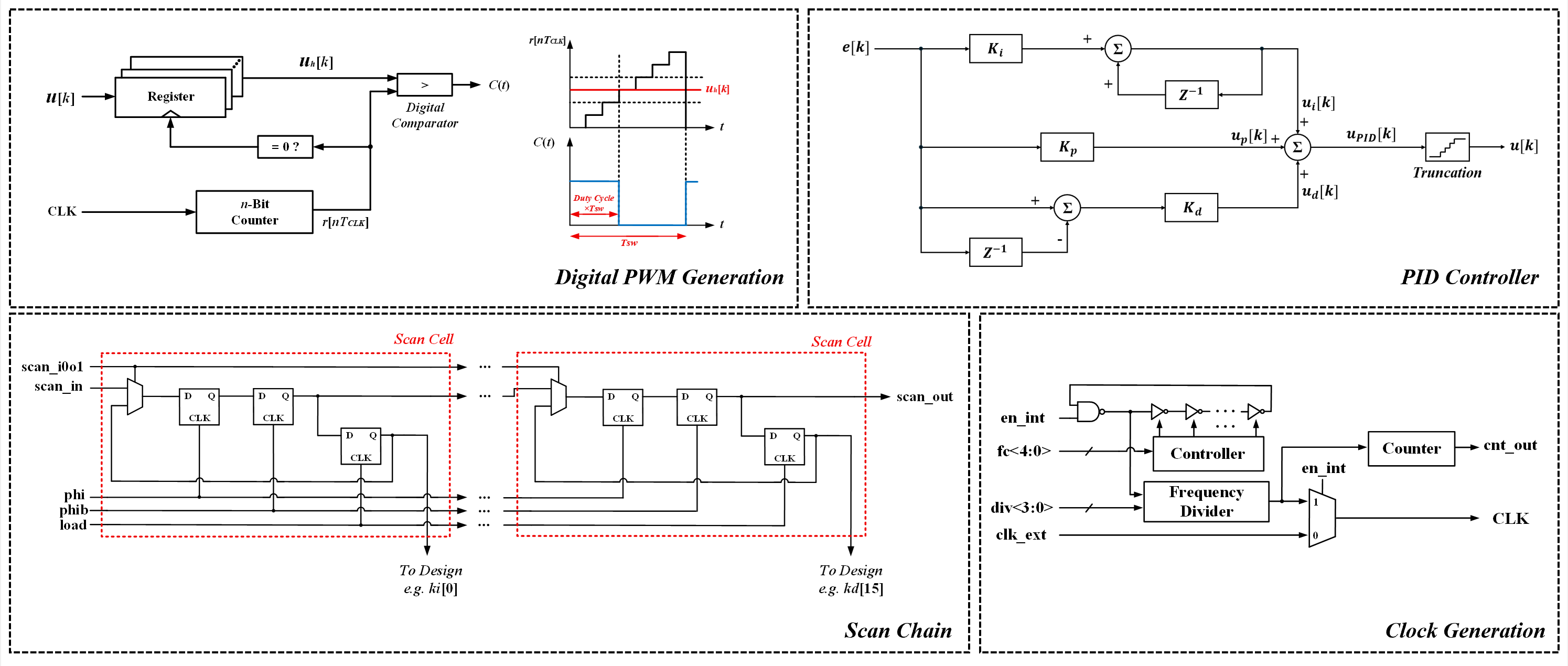
Scan Chain & Clock Generation
The scan chain is used to load the three PID coefficients (ki, kp, and kd) as well as other control bits into the digital controller. This serial-access mechanism enables flexible tuning, testability, and debugging during both pre-silicon verification and post-silicon evaluation without requiring additional dedicated I/O pins.
The ring–oscillator–based clock generation block provides a 64MHz on-chip clock, which is distributed to both the ADC and the DPWM. The use of a ring oscillator enables fully integrated, compact, and low-power clock generation without requiring any off-chip components. The generated 64MHz clock ensures synchronized operation between the sampling process in the ADC and the switching control in the DPWM, supporting consistent timing for the entire digital control loop.
Design Flow
Because our project is a mixed-signal design, multiple EDA tools are utilized throughout the entire design flow.
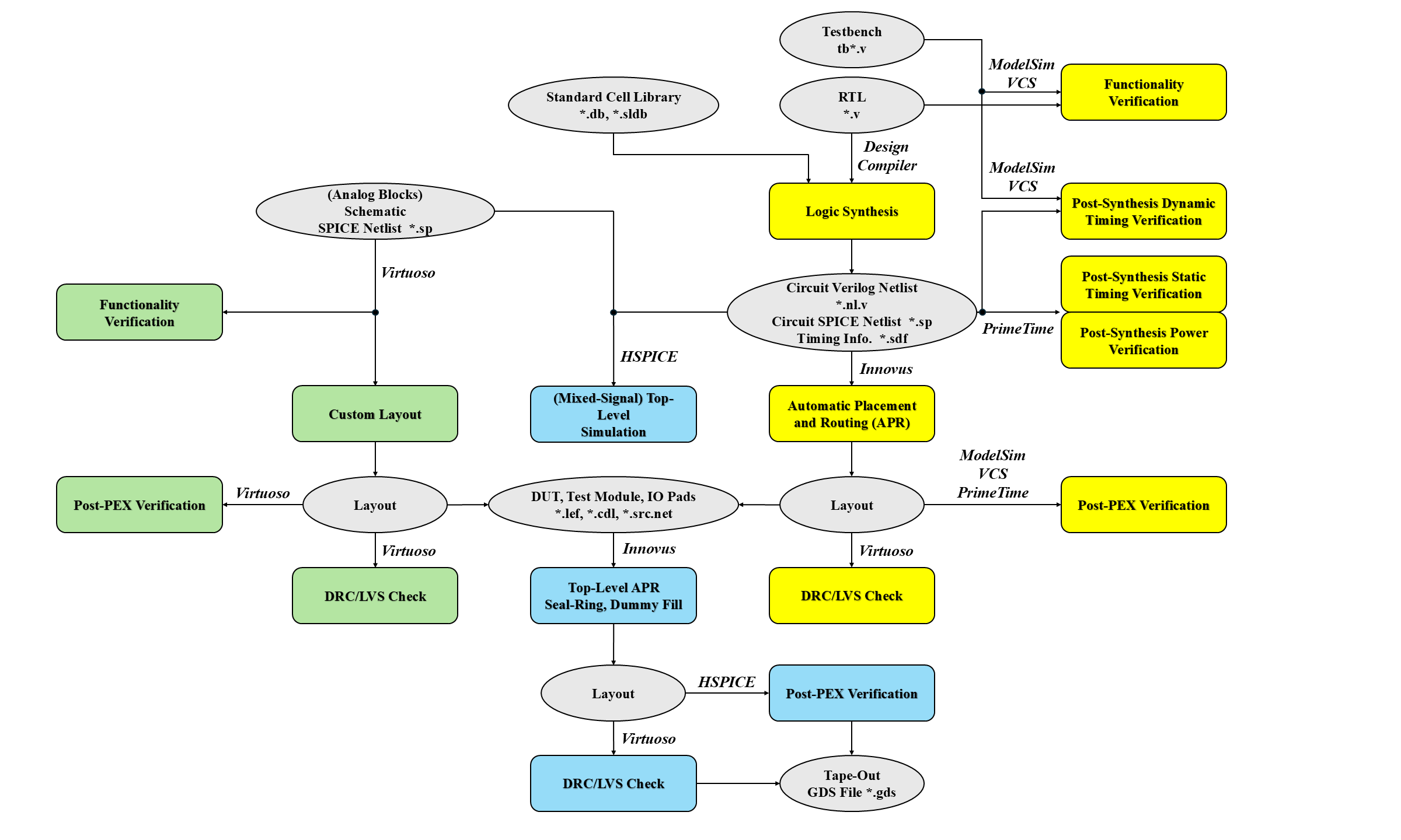
Schematic and RTL Design
The analog blocks were designed in Cadence Virtuoso and verified using Spectre simulations to evaluate functionality and performance. The digital blocks were implemented using Verilog RTL, synthesized with Synopsys Design Compiler, and verified through ModelSim, PrimeTime, and VCS for functional correctness, timing closure, and power analysis.
For the mixed-signal top-level closed-loop simulation, HSPICE is used. The analog top-level netlist is extracted from Virtuoso, and the digital top-level Verilog netlist is converted into a SPICE-compatible format through custom scripting. These two domains are then integrated in a separate top-level SPICE netlist, which is used to perform the full mixed-signal closed-loop simulation and validate the overall system behavior.
Physical Design
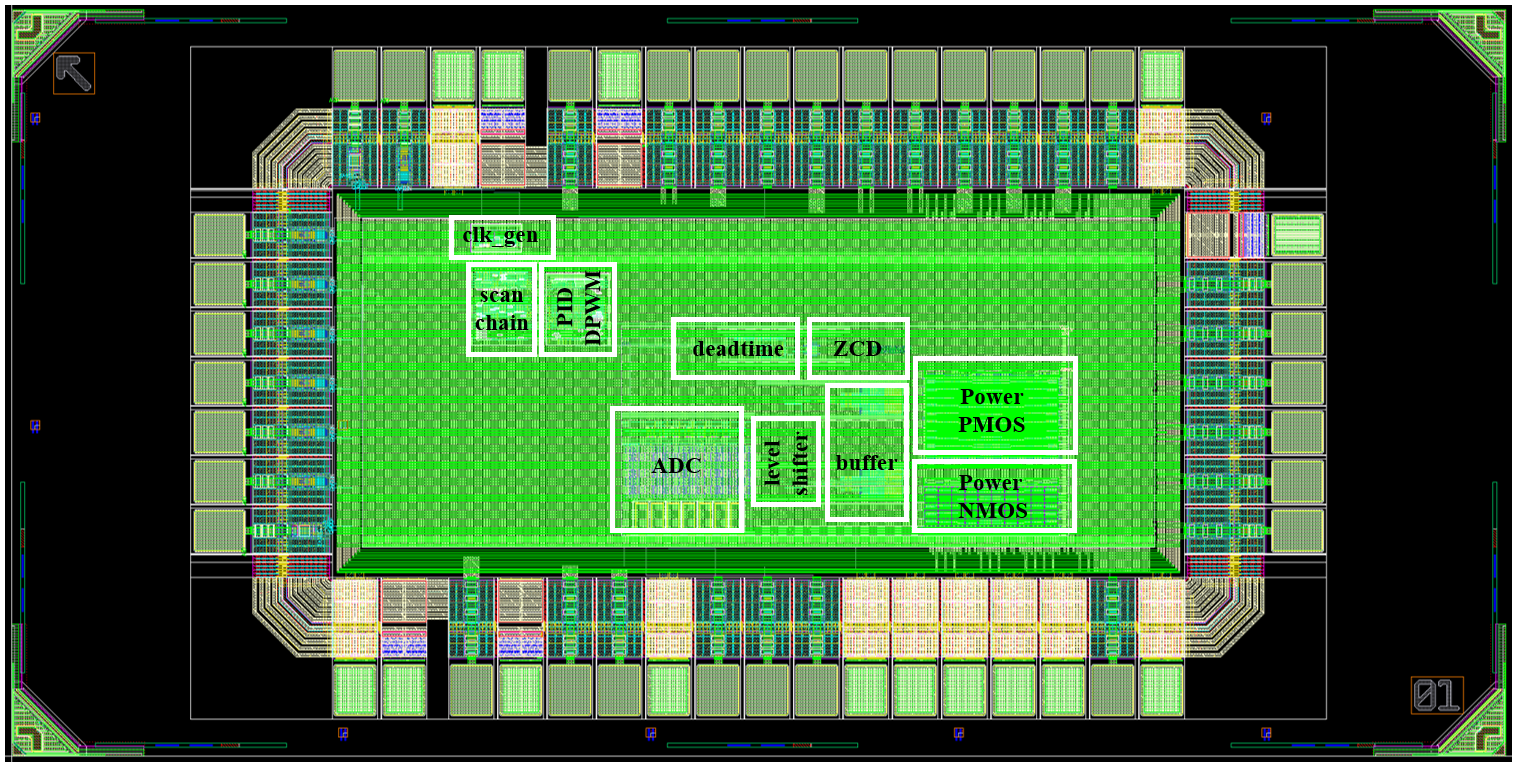
The floor plan is shown as follows:
The layouts of the analog blocks are designed in Cadence Virtuoso, after which LEF files are extracted. The layouts of the digital blocks and the test block are generated using automatic placement and routing (APR) in Cadence Innovus.
The top-level layout (excluding I/O pads) is implemented in Cadence Innovus using APR. Subsequently, the I/O pads, seal ring, and dummy fill (to resolve density violations) are added in Innovus through APR. This completes the chip-level layout, after which the GDSII file is generated and submitted to the fabrication foundry for tape-out.
The final chip-level layout is shown as follows:
Testing & Verification
This section presents the overall verification and validation flow used to ensure the correct functionality of the buck converter chip. The testing process is divided into pre-silicon verification, which confirms circuit functionality before tape-out, and post-silicon validation, which evaluates the fabricated chip under real measurement conditions.
Post-Layout Simulation
Digital Blocks
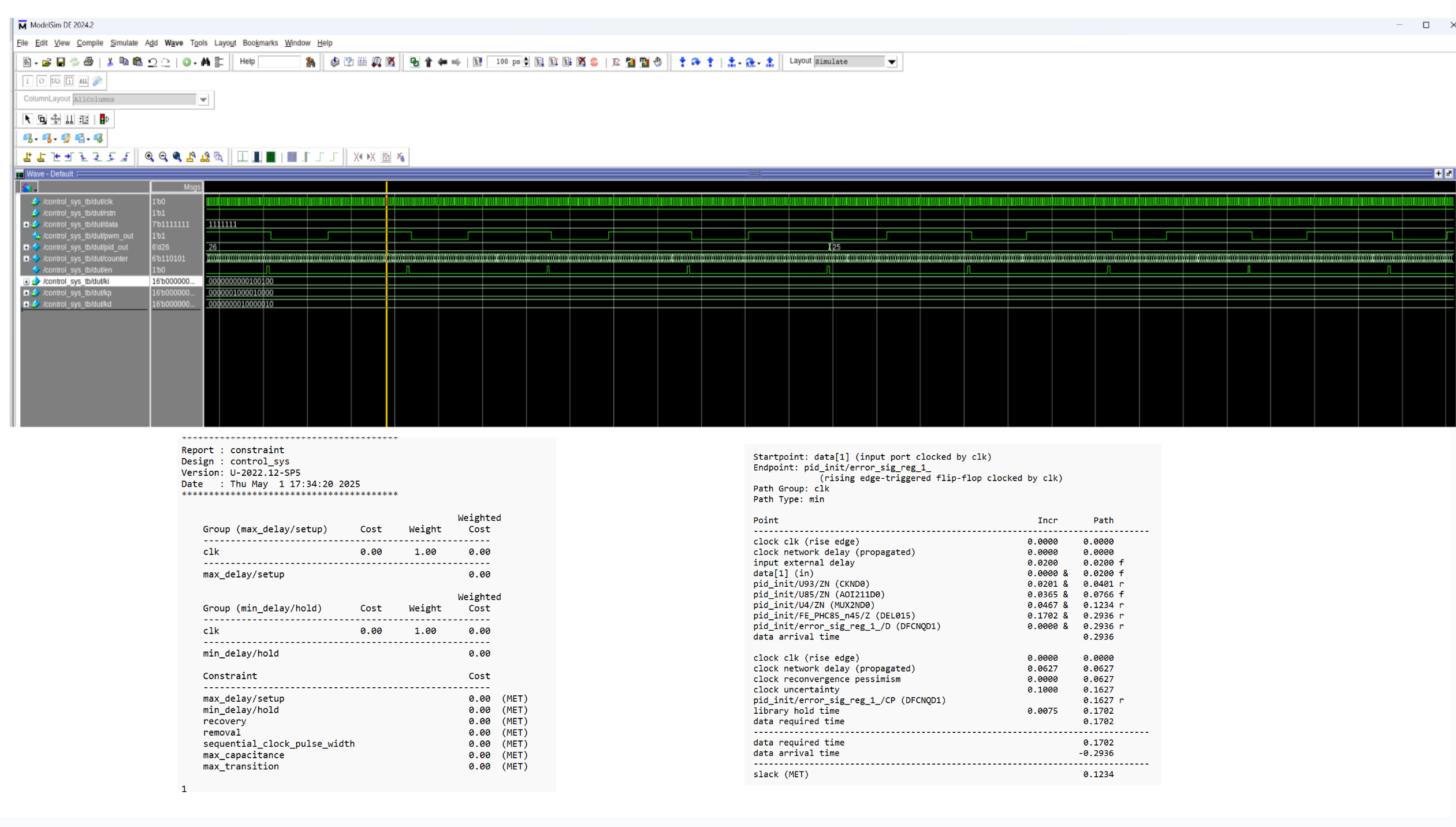
To verify the correctness of the digital control logic, comprehensive testbenches were written in Verilog for each module and for the combined digital top. Simulations were run in ModelSim, both before synthesis (RTL) and after synthesis (gate-level), to detect potential timing issues introduced by the synthesis process. In addition, Static Timing Analysis (STA) was conducted in Synopsys PrimeTime to verify that all timing constraints were met and to ensure that the design operated reliably at the target clock frequency. The figure below shows the ModelSim simulation waveform alongside a snapshot of the PrimeTime timing report.
Analog Blocks
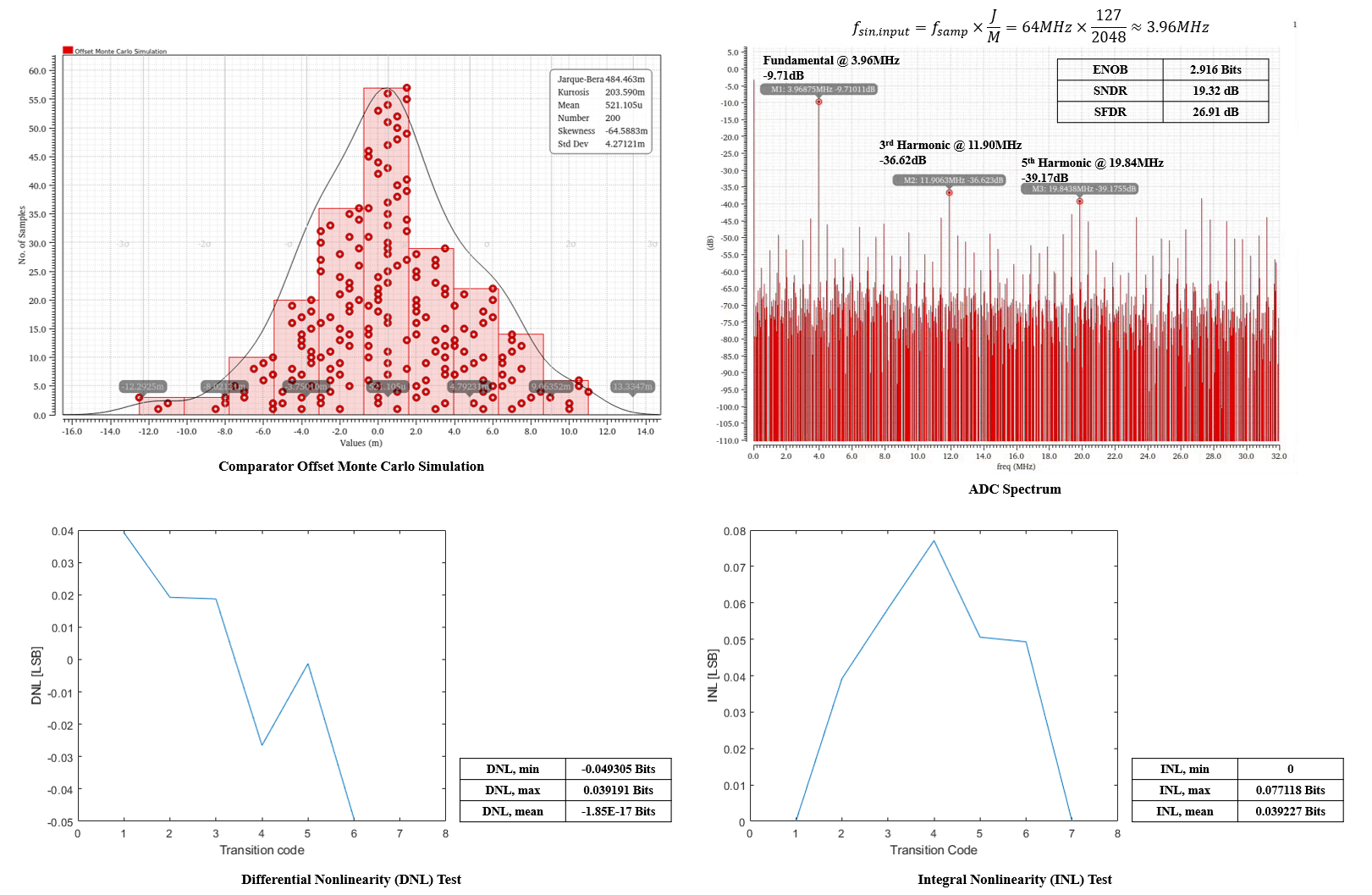
Here, we present post-layout simulation results of several analog blocks, including the ADC and the comparators. For the comparators, Monte Carlo simulations were performed to evaluate the input-referred offset. For the ADC, spectral analysis was conducted to extract key performance metrics such as ENOB, SNDR, and SFDR. In addition, the ADC’s dynamic linearity was characterized through DNL and INL simulations.
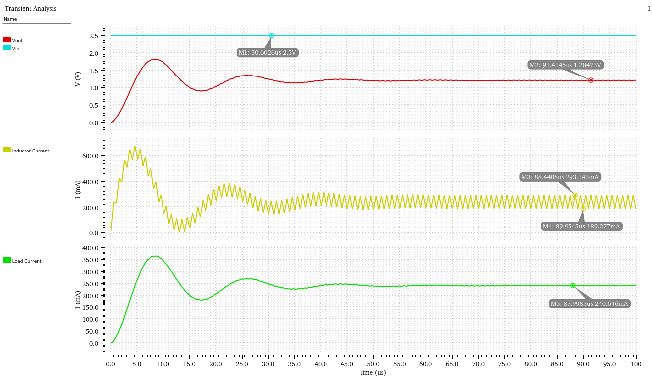
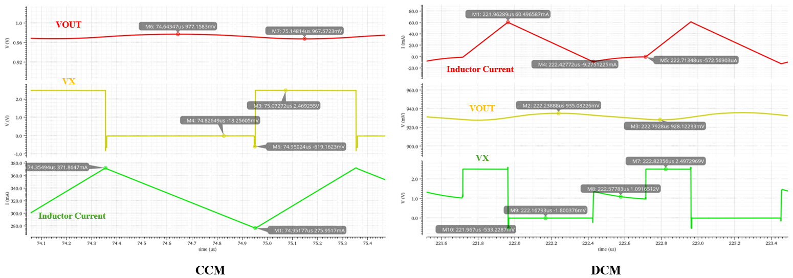
Top-Level
To verify the design after the place-and-route (PnR) and I/O pad integration stages, static timing analysis (STA) was performed using PrimeTime, and the digital functionality was verified in ModelSim using dedicated testbenches. Since the integrated design includes analog blocks that cannot be meaningfully analyzed using digital static timing analysis or simulated using standard digital HDL simulators such as PrimeTime and ModelSim, a behavioral Verilog model was created to replace the analog top during post-PnR digital verification. This model serves as an interface bridge between the digital blocks, enabling post-PnR timing verification and functional simulation to be carried out using standard digital design tools.
The top-level post-layout simulation is also based on HSPICE, and the results are presented below.
Post-Silicon Validation
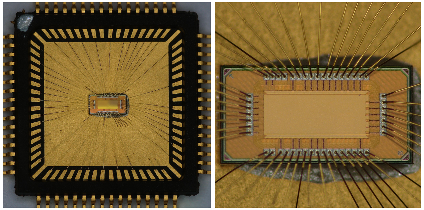
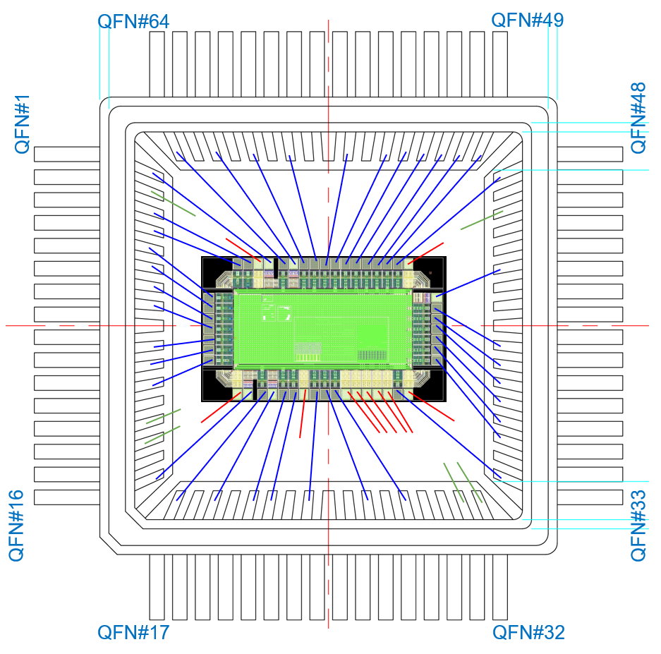
After fabrication, the initial bring-up of the chip was performed using a breadboard-based test setup. The chip was mounted in a QFN-64 socket and connected to the breadboard via jumper wires, enabling basic functionality checks and early debugging.
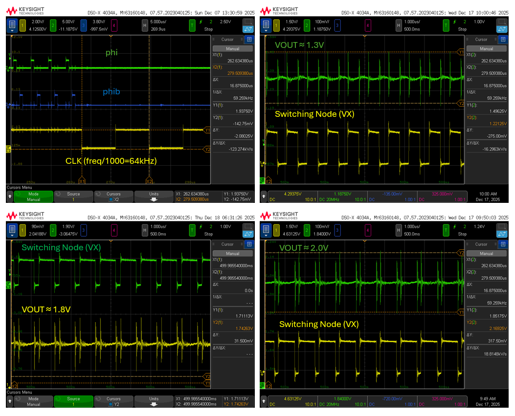
A custom PCB was subsequently designed to provide a stable testing environment. The PCB interfaces the chip with an Xilinx FPGA, which programs the digital control parameters and clock configuration through the on-chip scan chain. The PID coefficients and clock settings are set in MATLAB and serialized into the chip via the FPGA. Supply and reference voltages are verified using a digital multimeter before operation. Key signals, including the non-overlapping scan-chain clock(phi and phi_b), the clock, the switching node voltage (Vx), and the output voltage (Vout), are probed with an oscilloscope to evaluate timing, switching behavior, and closed-loop regulation, as shown in the following figures.
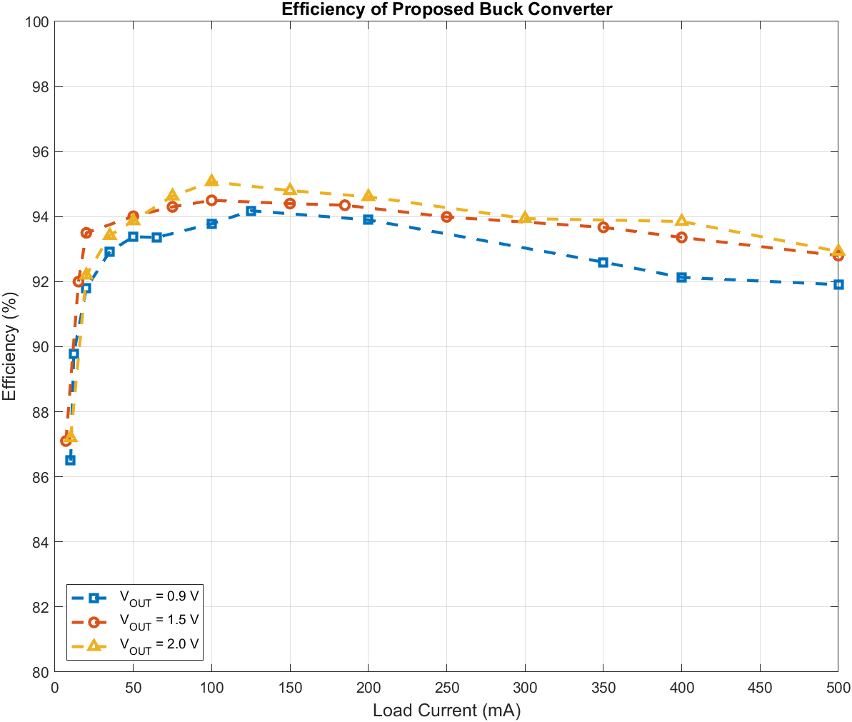
The efficiency results (both CCM and DCM) when the VOUT is 0.9V,1.5V, and 2.0V are shown as follows. The peak efficiency is nearly 95%, and the DCM efficiency is always above 85%.
PCB Design
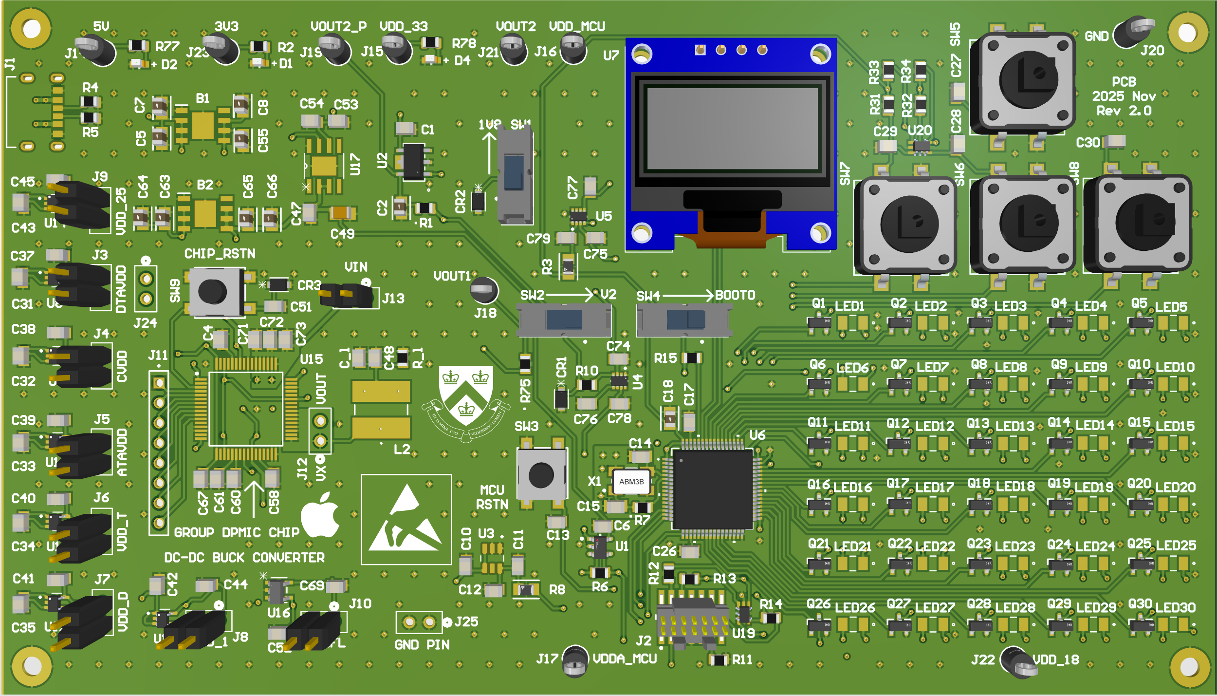
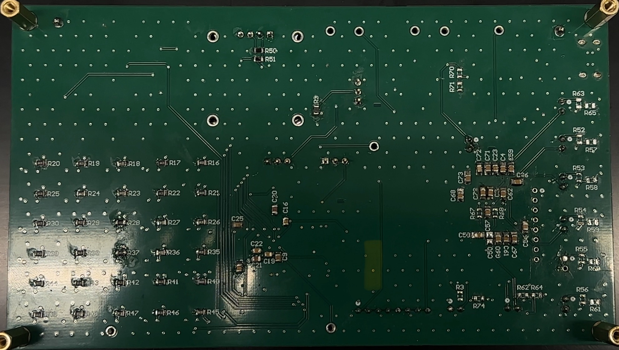
To demonstrate the functionality of our chip, we designed a 4-layer PCB using Altium Designer.
Schematic Design
Power Supply
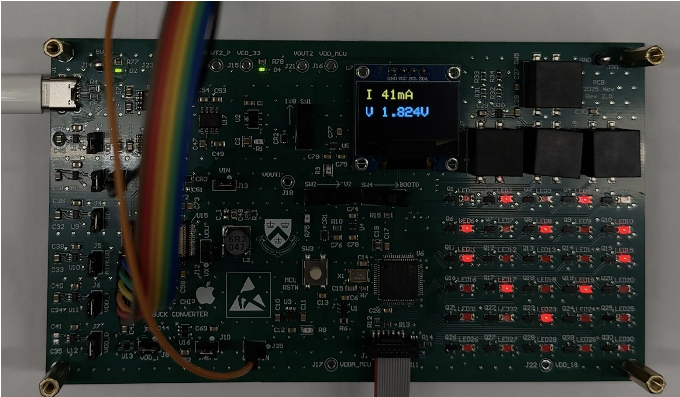
The board is powered through a USB Type-C connector, which supplies 5 V from either a wall adapter or a portable power bank. Several LDOs then regulate the 5 V rail down to the voltages required by both the demo circuits and our chip.
Power-indicator LEDs are included to provide visual feedback of active rails.
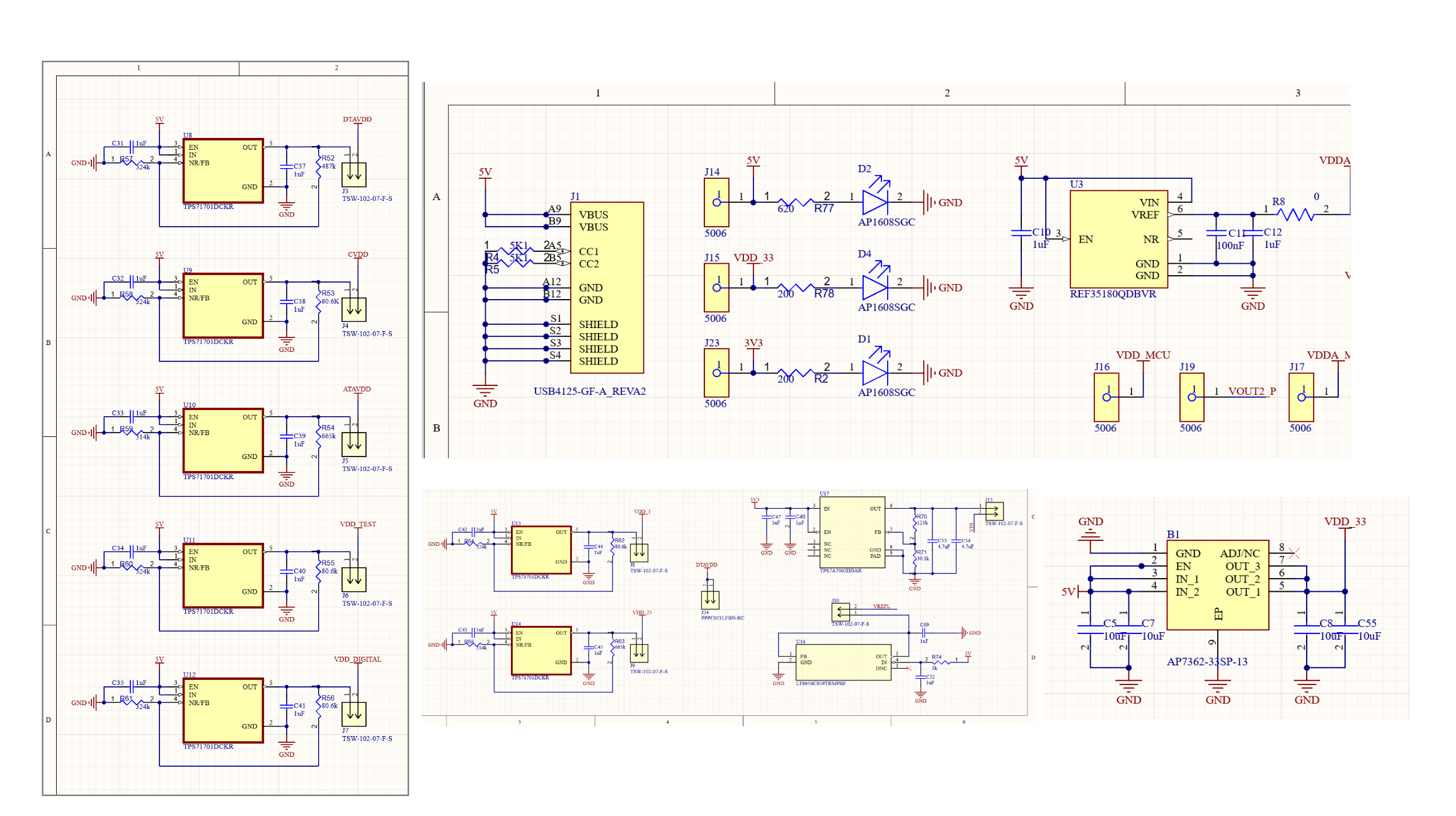
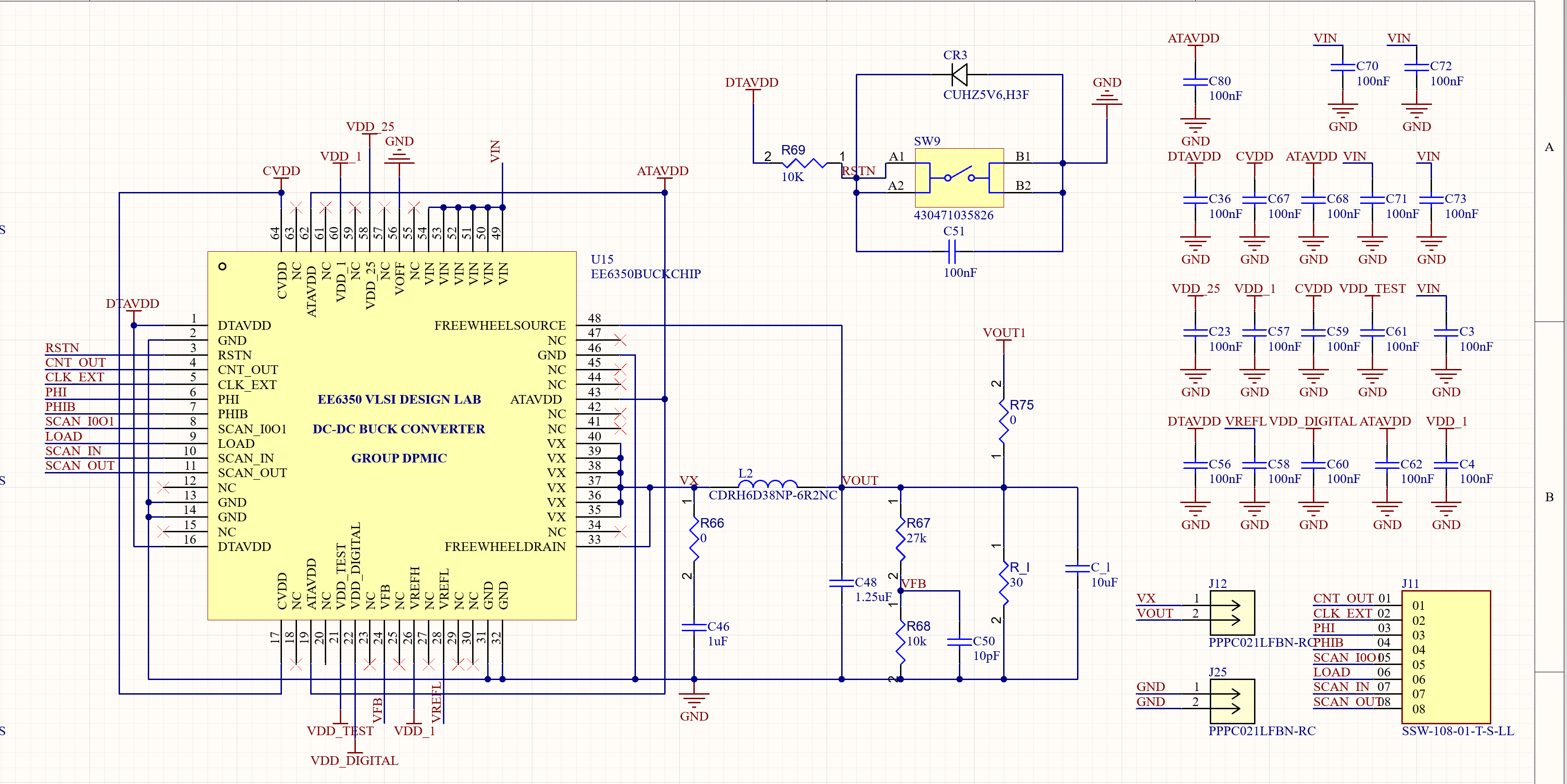
Buck Converter Circuit
The figure below shows the supporting circuitry for our buck converter chip. Note that a resistor divider is placed at the output of the chip, providing feedback voltage to the chip.
A tactile switch is included to reset the digital module, and an ESD protection diode is added to prevent static discharge from damaging the chip.
The 100nF ceramic capacitors are added accordingly for local decoupling.
An 8-pin header is added for scan-chain access, with two additional headers reserved for debugging.
STM32 MCU
An STM32 MCU is integrated on the board to run our demos. Its support circuitry includes a 16 MHz crystal oscillator, boot-configuration components, and an ST-LINK programming connector.
A power multiplexer allows the MCU to be powered from different voltage sources, selectable through a slide switch.
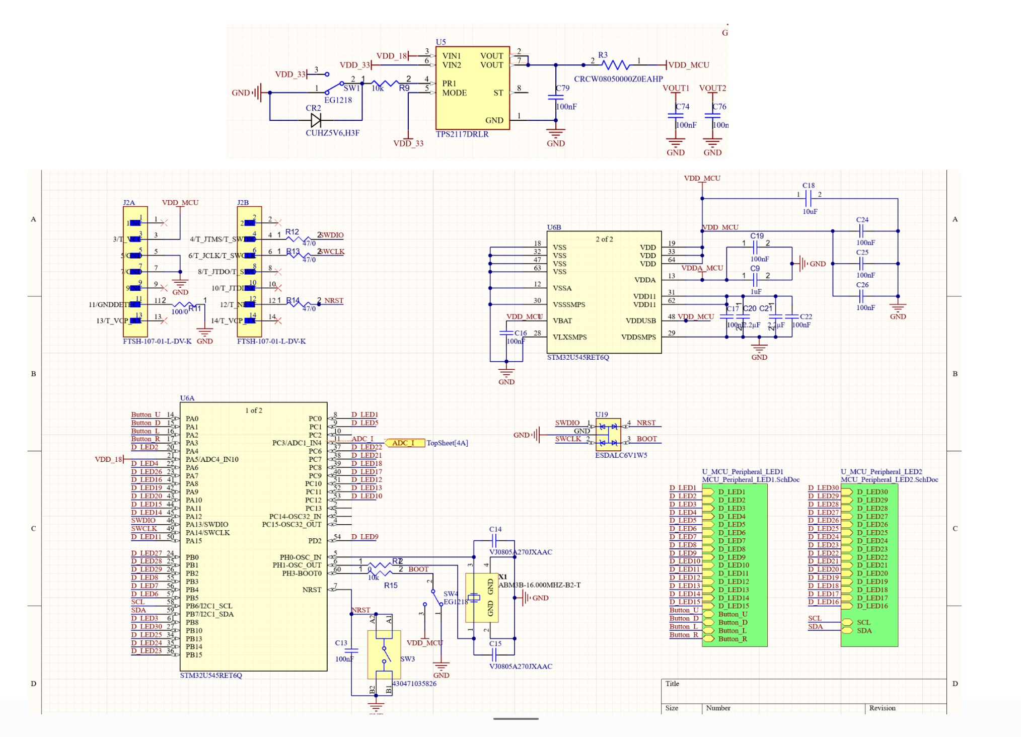
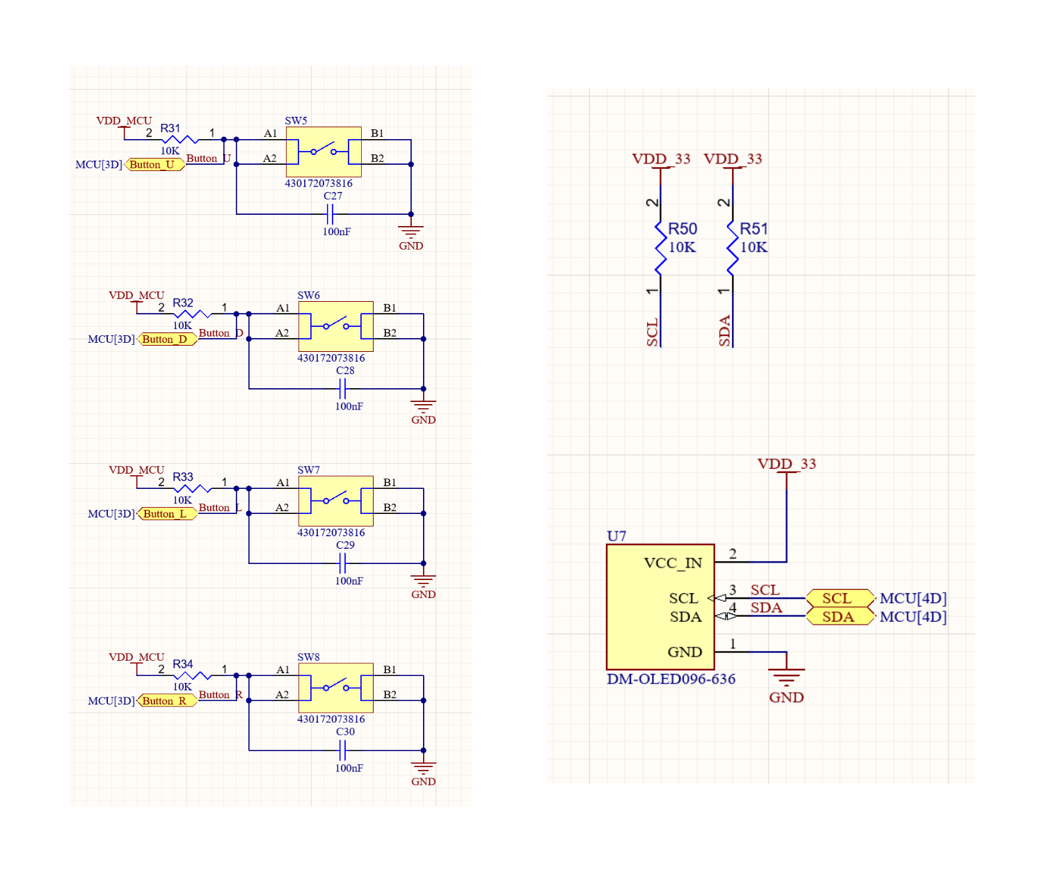
OLED Display & Buttons
An OLED screen is added to the PCB board for displaying. It communicates with the MCU through the I²C interface, with two 5.1 kΩ pull-up resistors included on the SDA and SCL lines.
Four push buttons are included to allow users to switch modes and interact with the demo.
LED Array
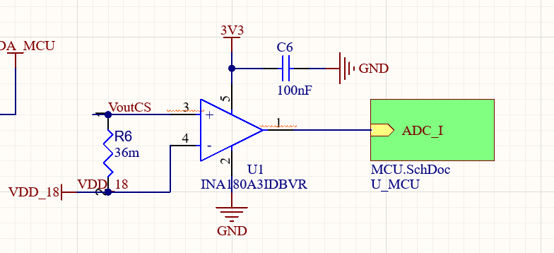
To monitor the output current of our chip, a high-side current-sensing amplifier measures the voltage across a precision sense resistor. The amplified output is fed into the STM32 for real-time display and logging.
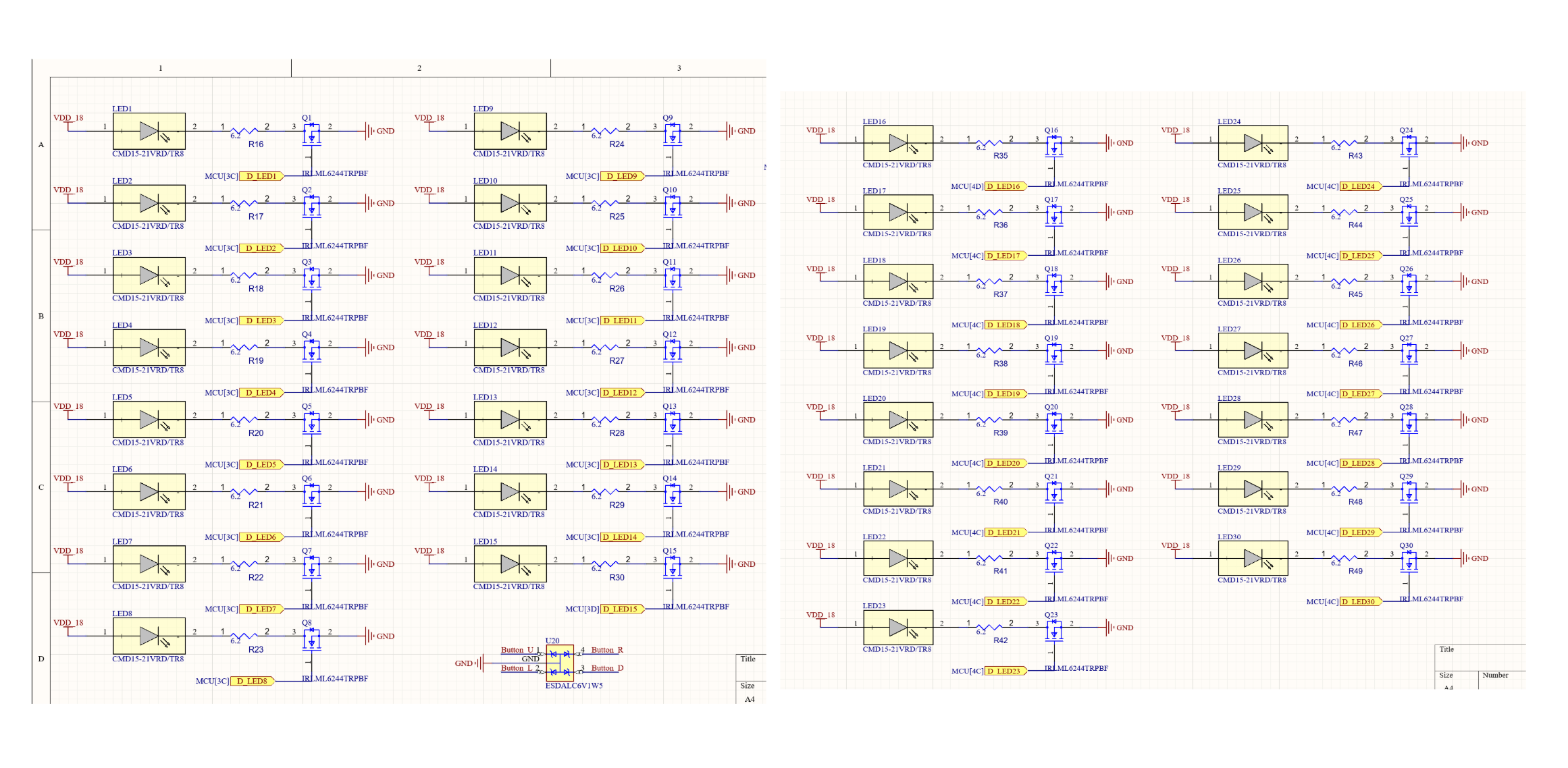
Current Sensing Amplifier
To demonstrate the functionality of our chip, we designed a 4-layer PCB using Altium Designer.
Layout Design
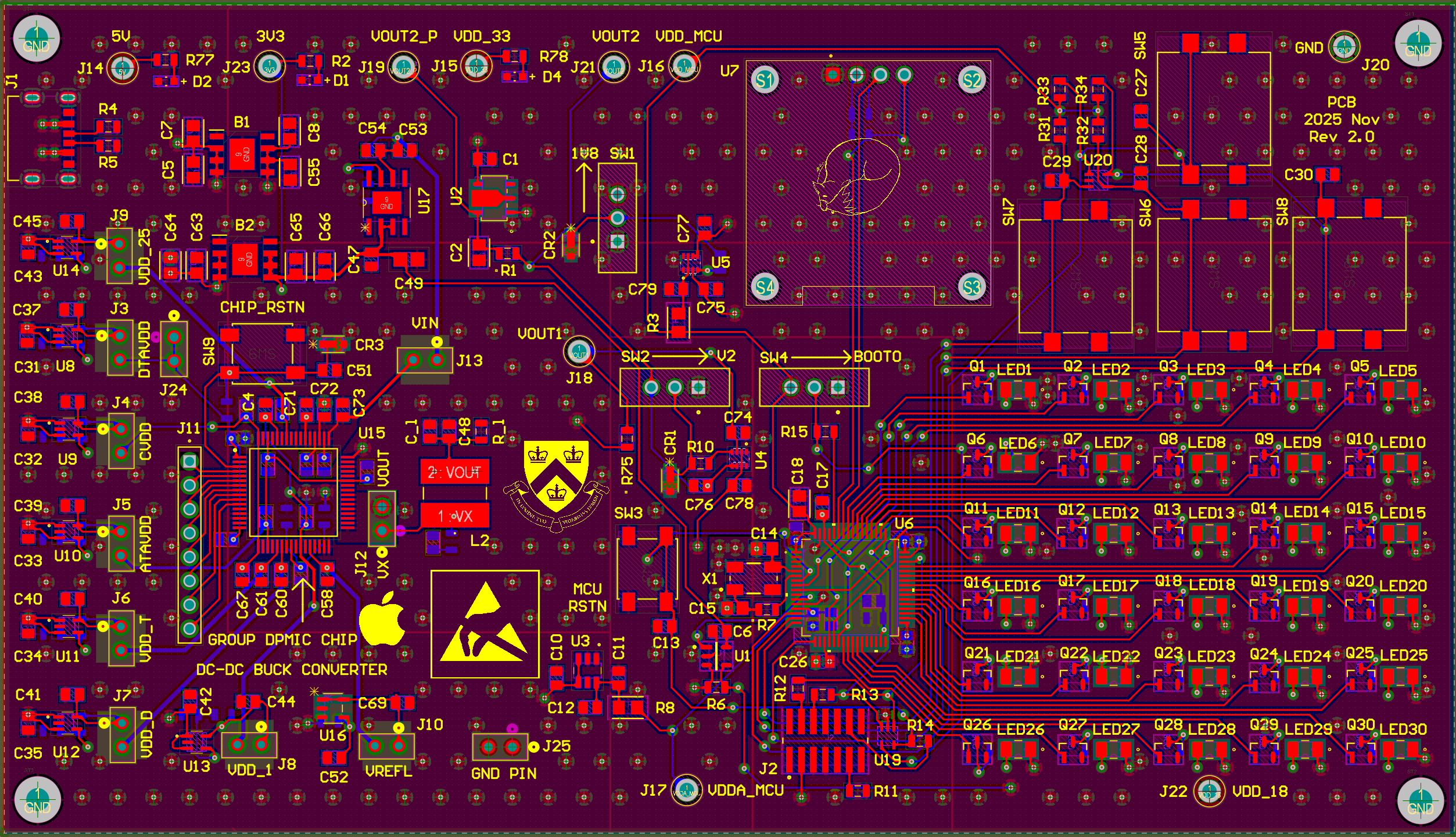
The figure below shows our layout design for the Demo PCB. The top and bottom layers are both signal layers, and the middle layers are the power and ground plane. We mainly used 10mil traces as our application does not require high current. Both outer layers include ground pours, and stitching vias connect all ground regions together to ensure low-impedance return paths.
Decoupling capacitors are placed as close as possible to the relevant IC pins to maximize their effectiveness.
Assembly
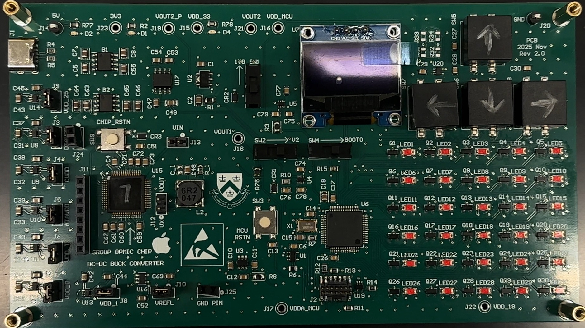
We used both a reflow oven and hand-soldering for the board assembly, and the images below show the assembled board.
Demonstration
The pictures below show two demonstration modes of our board: first, the chip supplies 1.8 V to the MCU while it runs a snake game; second, the chip powers the 1.8 V LED array. In both cases, the real-time output voltage and current provided by the chip are displayed on the OLED screen.
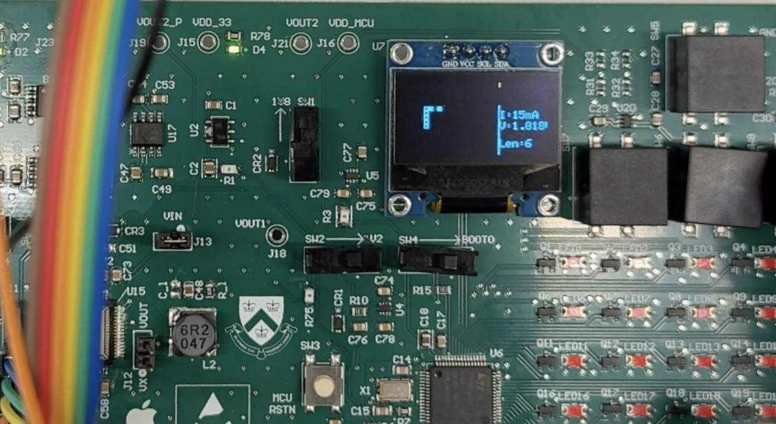
The basic idea of using a buck converter to power the LED array is to vary the load current by changing the number of LEDs that are turned on, while keeping the output voltage approximately constant. This is also a kind of load regulation.
The details are introduced in the following demo video.
Video Demonstration
Chip Specifications
The chip specifications are listed in the following table.
| Parameter | Specification |
|---|---|
| Technology | TSMC 65nm |
| Die Size | 2mm × 1mm |
| Input Voltage | 2.5V |
| Output Voltage | 0.9~2.0V |
| Supply Voltage | 1V core, 2.5V I/O |
| Maximum Load Current | 500mA |
| Output Voltage Ripple | 20~50mV |
| Current Ripple | ~100mA |
| Switching Frequency | ~1MHz |
| Package | QFN-64 |
Conclusions
Key Achievements
In our first tape-out experience, we successfully designed, implemented, and validated the proposed buck converter, leveraging knowledge from prior coursework and insights from the relevant research literature.
Throughout this project, we developed a deeper understanding of the key design trade-offs involved in power converter design, including efficiency, stability, transient response, and area constraints. In addition, we gained extensive hands-on experience with a wide range of EDA tools spanning digital IC design, analog IC design, and PCB design, covering the complete workflow from system-level architecture, circuit design and simulation, to layout, verification, and integration.
This tape-out experience significantly strengthened our ability to translate theoretical concepts into a manufacturable silicon implementation and enhanced our practical engineering skills in mixed-signal power management IC design.
Lessons Learned
Chip design is a highly demanding and multidisciplinary process that requires designers to possess both broad knowledge and practical experience. Designers should avoid narrowing their focus to a single domain and instead learn to approach problems from multiple perspectives. For example, analog designers can significantly enhance their design capability by understanding digital circuits, while digital designers can benefit from learning analog fundamentals.
Chip design and tape-out extend far beyond running simulations and observing waveforms. In real industrial practice, a robust design that functions reliably across PVT corners and achieves reasonable yield is often more valuable than sophisticated or aggressive circuit topologies that are difficult to manufacture or validate.
Chip layout is an art, especially in analog IC design. It demands careful consideration of matching, symmetry, parasitics, routing, and layout-dependent effects. Although the analog blocks in our project are not complex, achieving a clean, well-optimized layout remains a challenging, iterative process, underscoring the critical role of layout quality in overall chip performance.
Future Work
Future work can focus on hybrid control architectures for the buck converter, inspired by hybrid-controlled LDO designs. By incorporating an analog control loop into a digitally controlled buck converter, higher output voltage accuracy and improved transient performance can be achieved, while the digital control loop continues to provide flexibility and ease of compensation tuning.
Adaptive or self-calibrated control techniques can also be explored to adjust loop parameters across PVT corners automatically. For example, on-chip calibration of comparator offsets, ADC gain, or digital PID coefficients can further improve output accuracy and robustness without manual tuning, reducing sensitivity to process and temperature variations.
In addition, more comprehensive on-chip monitoring and protection circuits can be integrated to enhance system robustness and reliability. These may include over-current protection (OCP), over-voltage protection (OVP), under-voltage lockout (UVLO), and thermal protection, enabling safe operation across a wide range of load and environmental conditions.
References
- Lecture Notes, EE6340 Power Management Integrated Circuits, Prof. Xin Zhang, Columbia University in the City of New York, Fall 2024.
- Lecture Notes, EE6350 VLSI Design Lab, Prof. Mingoo Seok, Columbia University in the City of New York, Spring 2025.
- Lecture Notes, EE6316 Analog-Digital Interfaces in VLSI, Prof. Tod Dickson, Columbia University in the City of New York, Spring 2025.
- X. Zhang et al., “A 0.6 V Input CCM/DCM Operating Digital Buck Converter in 40 nm CMOS,” IEEE J. Solid-State Circuits, vol. 49, no. 11, pp. 2377–2386, Nov. 2014, doi: 10.1109/JSSC.2014.2339325.
- J. Baek, H.-M. Lee, and S.-U. Shin, “Triple-Mode Switched-Inductor-Capacitor DC-DC Buck Converter with Reusable Flying Capacitor and Bang-Bang Zero-Current Detector for Wide Load Current Range,” Electronics, vol. 9, no. 8, p. 1202, July 2020, doi: 10.3390/electronics9081202.
- Xuan-Dien Do, Seok-Kyun Han, and Sang-Gug Lee, “Low power consumption for detecting current zero of synchronous DC-DC buck converter,” in 2012 International SoC Design Conference (ISOCC), Jeju Island, Korea (South): IEEE, Nov. 2012, pp. 487–490. doi: 10.1109/ISOCC.2012.6406902.
- L. Corradini, D. Maksimović, P. Mattavelli, and R. Zane, Digital Control of High‐Frequency Switched‐Mode Power Converters, 1st ed. Wiley, 2015. doi: 10.1002/9781119025498.
- R. W. Erickson and D. Maksimović, Fundamentals of Power Electronics. Cham: Springer International Publishing, 2020. doi: 10.1007/978-3-030-43881-4.
- V. Michal, “Inductor Current Zero-Crossing Detector and CCM/DCM Boundary Detector for Integrated High-Current Switched-Mode DC–DC Converters,” IEEE Trans. Power Electron., vol. 29, no. 10, pp. 5384–5391, Oct. 2014, doi: 10.1109/TPEL.2013.2292600.
- Chi-Lin Chen, Wei-Jen Lai, Ter-Hsing Liu, and Ke-Horng Chen, “Zero current detection technique for fast transient response in buck DC-DC converters,” in 2008 IEEE International Symposium on Circuits and Systems (ISCAS), Seattle, WA, USA: IEEE, May 2008, pp. 2214–2217. doi: 10.1109/ISCAS.2008.4541892.
- P. Shukla, P. Singh, T. Maheshwari, A. Grover, and V. Rana, “A 800MHz, 0.21pJ, 1.2V to 6V Level Shifter Using Thin Gate Oxide Devices in 65nm LSTP,” in 2020 27th IEEE International Conference on Electronics, Circuits and Systems (ICECS), Glasgow, UK: IEEE, Nov. 2020, pp. 1–4. doi: 10.1109/ICECS49266.2020.9294984.
- B. Razavi, “The StrongARM Latch [A Circuit for All Seasons],” IEEE Solid-State Circuits Mag., vol. 7, no. 2, pp. 12–17, 2015, doi: 10.1109/MSSC.2015.2418155.
- B. Wicht, T. Nirschl, and D. Schmitt-Landsiedel, “Yield and speed optimization of a latch-type voltage sense amplifier,” IEEE J. Solid-State Circuits, vol. 39, no. 7, pp. 1148–1158, July 2004, doi: 10.1109/JSSC.2004.829399.
Acknowledgments
We want to thank everyone who supported us throughout this project and made this work possible.
We are especially grateful to our course advisor, Prof. Mingoo Seok, for giving us the invaluable opportunity to participate in this class and experience our first-ever tape-out. He proposed the project topic, met with us weekly to review our progress, and guided us with his technical expertise and extensive experience in chip design.
Special thanks go to Yichen Xu, who has a solid power management IC background and was consistently available to answer our questions and help us overcome critical challenges throughout the design process.
We also thank our teaching assistants, Mosom Jana, Da Won Kim, and Chuan-Tung Lin, for providing us with technical resources and insightful suggestions.
Finally, we would like to express our sincere appreciation to Apple Inc. for their generous support and sponsorship, without which this project would not have been possible. We further extend our gratitude to the Apple engineers who participated in our design reviews and offered invaluable feedback.
Team Members