Introduction
Our project is a fully integrated RISC-V-based SoC fabricated in TSMC 65 nm CMOS technology. The system is built around the OpenHW Group’s CORE-V CV32E40P RISC-V CPU core, connected through an AHB-based system bus with an AHB-to-APB bridge to access a rich set of on-chip peripherals.
The SoC integrates instruction memory, data memory, SPI, UART, eight GPIOs, and two programmable timers, along with an on-chip clock generator, a debug finite-state machine, and a scan chain for DFT. We carried the project end-to-end: proposal, architecture design, RTL implementation and verification, synthesis, physical design and signoff (including STA), and finally PCB design, bring-up, and system-level validation. The final chip runs on hardware and passes our functional demo.
RTL, verification, PnR, STA, signoff, and PCB bring-up were executed end-to-end by the team.
Scan loads IMEM/DMEM, steps the clock, and reads back results for silicon debug.
Configurable fc/div controls feed the debug FSM for scan, run, and single-step modes.
SPI-driven display, UART prints, GPIO, and timers all validated on the custom PCB.
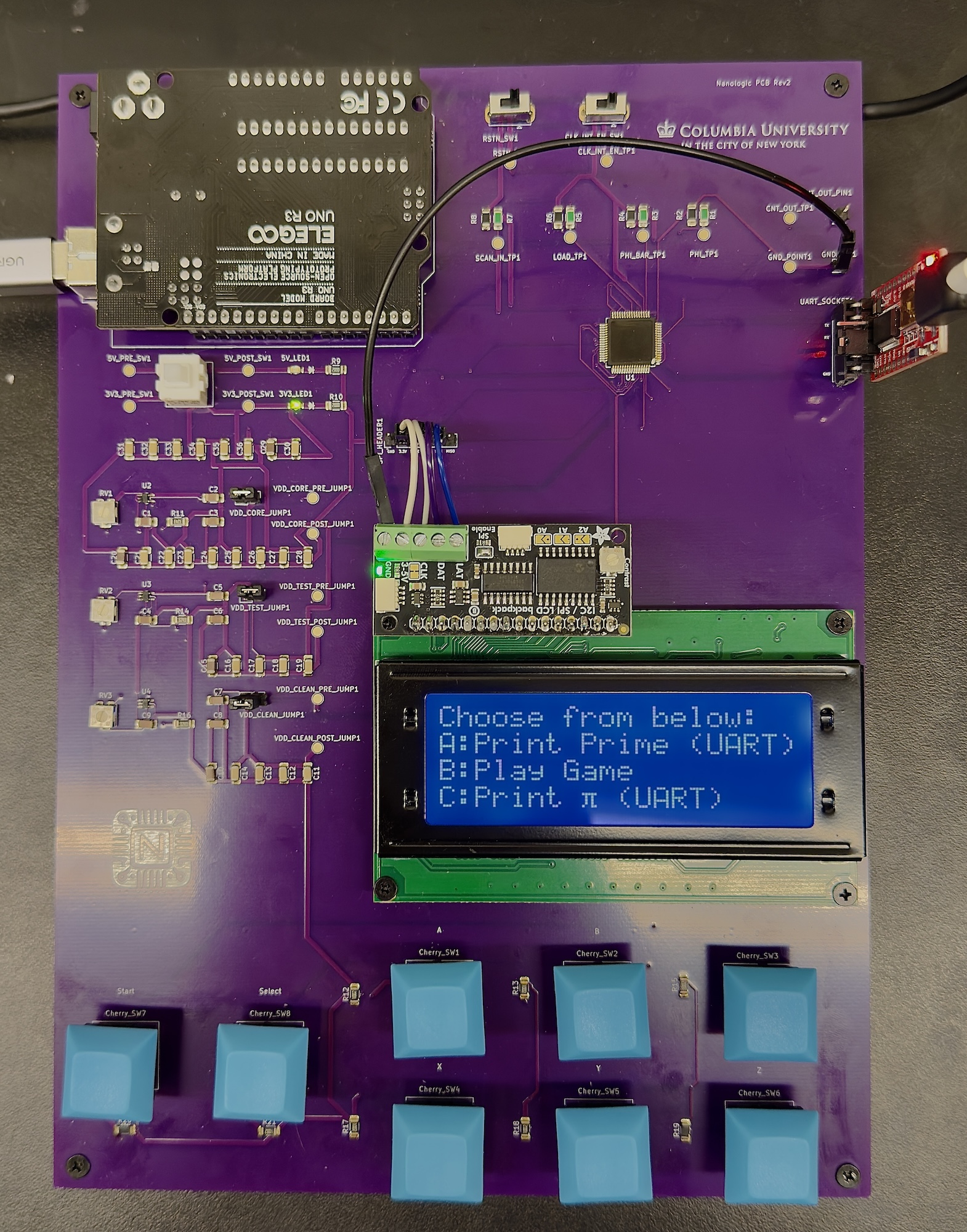
Whole System on PCB
System Architecture
The SoC adopts a modular architecture organized around a RISC-V CPU core, an AMBA-based interconnect, and a set of memory-mapped peripherals, memory and infrastructure blocks. All components are integrated within a compact 2 mm² die implemented in TSMC 65 nm CMOS technology.
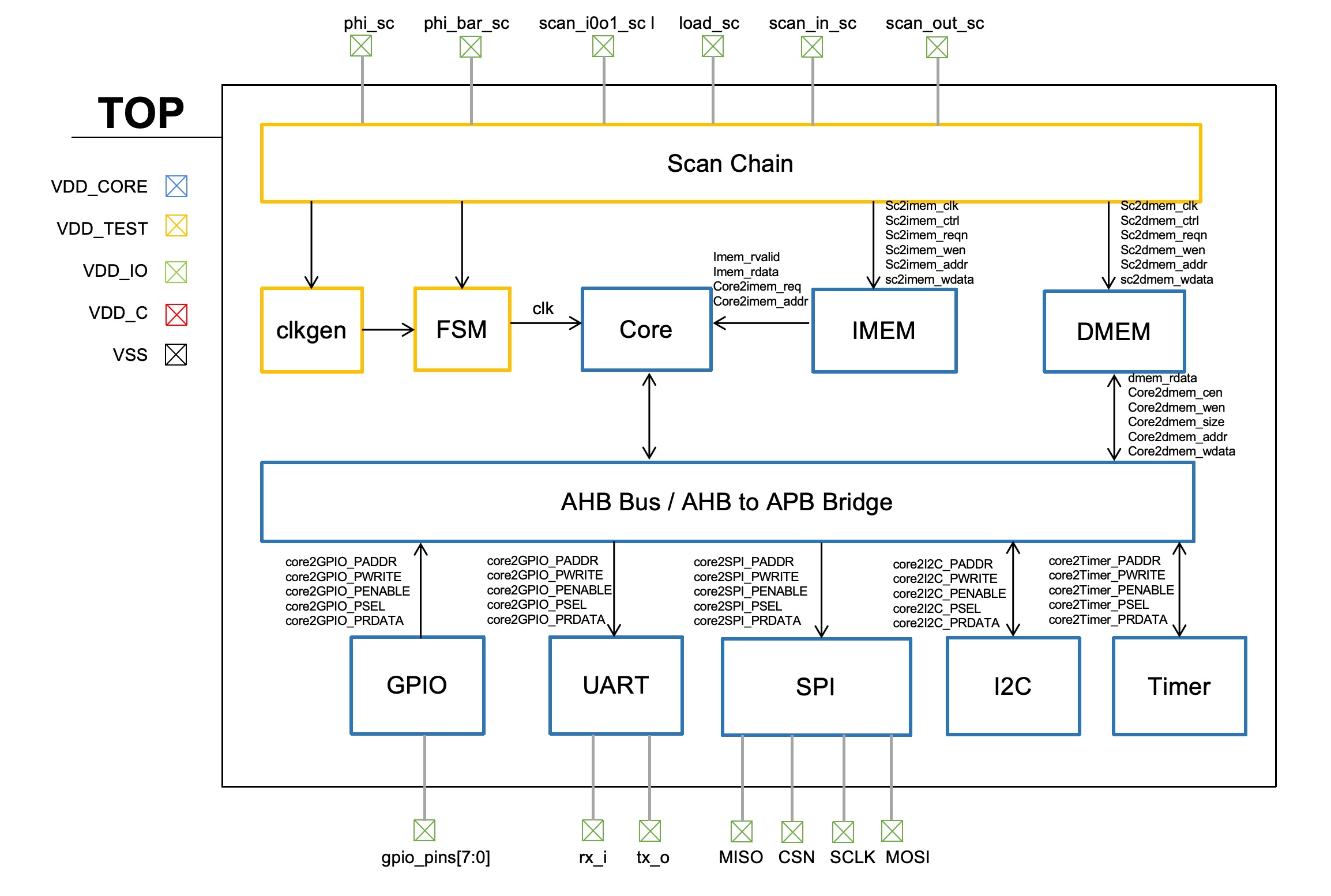
SoC Chip Block Diagram
Main Components
CPU
At the heart of the chip is our RISC-V CPU core, which executes all application and control software and serves as the sole bus master in the system. The core interfaces with the on-chip interconnect through a lightweight AHB master port, giving it unified access to data storage and all memory-mapped peripherals. Importantly, instruction memory (IMEM) is not accessed through the AHB bus; instead, it is directly connected to the CPU core. This dedicated instruction-fetch path simplifies timing and reduces bus traffic.
The CPU used in this project is version 1.8.3 of the OpenHW Group's RISC-V Core CV32E40P [1]. This core has been previously taped out as part of OpenHW's CORE-V MCU Development Kit; version 1.8.3 has undergone both formal verification and synthesis-based verification across multiple configurations, making it a mature and reliable open-source processor choice.
The CV32E40P is a 32-bit, in-order, 4-stage pipeline processor implementing RV32I, RV32M, RV32C, and either the RV32F or RV32Zfinx instruction set. It also supports the PULP custom extensions for enhanced performance.
For our project, we selected the RV32Zfinx variant, which reuses the general-purpose register file for floating-point operations instead of requiring a dedicated floating-point register file, making it significantly more area-efficient than RV32F. During early front-end architecture planning, we initially enabled floating-point support and intended to include the FPU. However, during the physical design phase, we identified significant challenges with timing closure and area overhead introduced by the FPU. Since floating-point computation was not essential to our intended functionality or demo, we ultimately disabled floating-point hardware support to ensure a more robust, compact, and timing-clean implementation.
CV32E40P Core
The CPU shown in the diagram is based on the CV32E40P core, a 4-stage, in-order RISC-V processor optimized for embedded and low-power applications. Its microarchitecture consists of the classic IF, ID, EX, and WB pipeline stages, with tightly integrated control logic to manage instruction flow, hazard resolution, and power-saving modes. The front end includes a prefetch buffer, instruction aligner, and compressed instruction decoder to improve instruction delivery efficiency. The register file and decoder feed multiple execution units, including an ALU, multiplier/divider, CSR unit, and an optional floating-point unit, enabling a wide range of integer and arithmetic operations. A dedicated Load-Store Unit (LSU) handles memory accesses and interacts with the external data interface. The core also integrates specialized units such as hardware loop registers, a debug interface, an interrupt controller, and a sleep unit for fine-grained power management. Overall, the design delivers a compact, configurable, and energy-efficient RISC-V processing solution suitable for microcontroller-class systems.
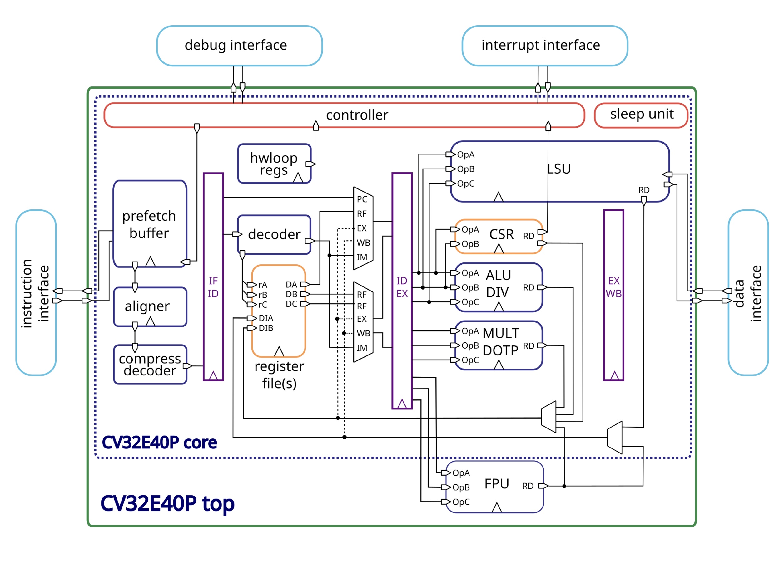
CV32E40P CPU Core
Clock Gating
CV32E40P uses a clock-gating strategy at the top level to reduce dynamic power consumption. Implementers define the specifics of clock gating for synthesis; rather than implementing custom gating logic, we used the clock-gating cells provided by TSMC.
At the top level, the clock network is divided into several functional domains. Each domain receives a gated clock through an ICG cell, and the enable signal is generated based on the activity of the corresponding module. When a module is idle, its clock is disabled, effectively reducing unnecessary switching activity.
The ICG cell integrates a latch and gating logic to ensure glitch-free clock gating and includes a test-enable input for scan and DFT support. Using this standard, fully characterized cell guarantees safe operation and seamless integration with synthesis, CTS, and STA.
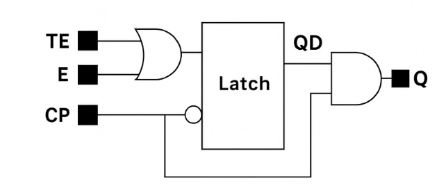
Clock Gating Cell
FPU
We originally planned to integrate an FPU into the SoC and successfully completed the compiler and linker configuration required to support floating-point operations. The FPU passed our initial functional simulations and worked correctly at the RTL level. However, after synthesis, physical design, and timing analysis, the FPU ran into timing issues that were not easily resolved. To maintain overall system stability and achieve a higher operating frequency, we ultimately decided to remove the FPU. Without the FPU's long combinational paths, the SoC's minimum achievable clock period improved from 15 ns to 5 ns, resulting in substantially better performance and a more reliable design.
Floating-point Unit (FPU)
Memory
The SoC adopts a Harvard memory architecture, with fully separated instruction and data memories to maximize throughput and simplify timing. The memory subsystem consists of two on-chip SRAM blocks:
- Instruction Memory (IMEM): Directly connected to the CPU instruction-fetch interface.
- Data Memory (DMEM): Exposed as an AHB slave and accessed by CPU load/store instructions.
The instruction memory provides a dedicated, point-to-point connection to the CPU's instruction-fetch interface. By avoiding the system bus entirely, IMEM enables deterministic instruction delivery, lower latency, and reduced bus contention. Originally, the design targeted 32 KB of instruction storage, but due to strict die-area constraints during physical design, the IMEM size was adjusted to 16 KB, which still meets the needs of our target workloads and demo applications.
The data memory is implemented as an AHB slave and connected to the CPU via the shared bus. All load/store instructions are routed through this bus interface, maintaining a clean separation between instruction fetch and data access. Similar to IMEM, DMEM was initially planned as 32 KB, but was downsized to 16 KB to fit within the allowable silicon footprint.
Addressing and byte enables
One important detail about both IMEM and DMEM is that, at the memory-macro level, each address corresponds to a 32-bit word. For 16 KiB of capacity, this yields a 12-bit word address bus. However, the RISC-V ISA is byte-addressed, so we provide a 4-bit byte-enable (BEN) bus (called WEN by the memory macro) that controls which bytes of the 32-bit word at a given address are actually written.
This integrates cleanly with the CPU, since it naturally provides the write size in bytes, which maps directly to the BEN bus. However, both the CPU and the AHB bus still generate byte addresses. To reconcile this with the word-addressed SRAM macros, we shift addresses right by 2 in two places: (1) for the scan chain, the memory wrappers shift the incoming address to force word alignment; and (2) for functional accesses, the IMEM wrapper shifts the AHB address, while for DMEM the shift is handled in the DMEM AHB slave.
Our peripherals, with the exception of UART, also treat memory addresses as byte-addressed and shift internally to reach word-aligned register addresses. The UART peripheral expects word-aligned addresses, so we shift its incoming address right by 2.
The key takeaway is that from the perspective of the CPU, the AHB bus, and the software, addresses are byte-based (with 32-bit alignment enforced by the compiler). From the perspective of the SRAM macros, addresses are word-based, and byte enables select which bytes within a word are updated.
SRAM Implementation and Memory Wrapper
Both IMEM and DMEM are implemented as SRAM hard macros generated with the ARM memory compiler. Since these macros are technology-specific and lack native support for system-level protocols or scan operations, we designed custom memory wrapper modules to ensure clean integration into the SoC.
The memory wrappers provide several key functions:
- Adapt the SRAM macro interfaces to the CPU and AHB protocol requirements, including read/write enables, chip select, and byte enables.
- Implement a dedicated mode-switching mechanism that supports both run mode and DFT scan mode.
- Add delay cells as needed to prevent hold-time violations.
- Provide a clean, synthesizable interface for RTL simulation while isolating technology-specific macro details.
Run Mode
In run mode, the wrapper exposes the memory as part of the functional SoC:
- IMEM connects directly to the CPU's instruction-fetch interface.
- DMEM operates as an AHB slave, servicing all CPU load/store requests via the system bus.
- All functional address, control, and data signals drive the SRAM in this mode.
Scan Mode
To enable complete chip-level scan coverage, the wrappers include logic that reconfigures the memory into scan mode during DFT operation:
- The memory wrapper becomes part of the SoC's continuous scan chain, enabling scan vectors to be shifted in and out.
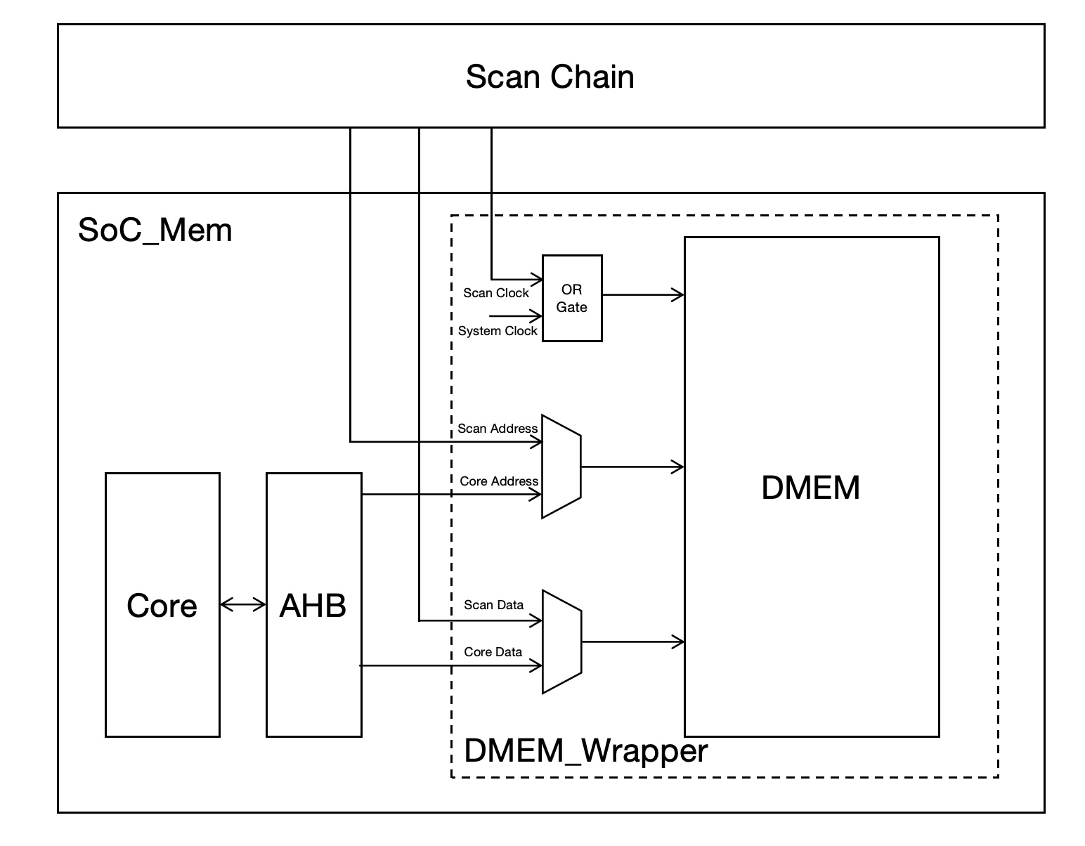
DMEM Wrapper
On-Chip Interconnect and Bus Architecture
A central AMBA AHB system bus forms the primary communication backbone of the SoC. The bus is organized in a 1-master/6-slave (M16S) topology, with the RISC-V CPU core acting as the only AHB master. This keeps the interconnect simple, low-latency, and area-efficient.
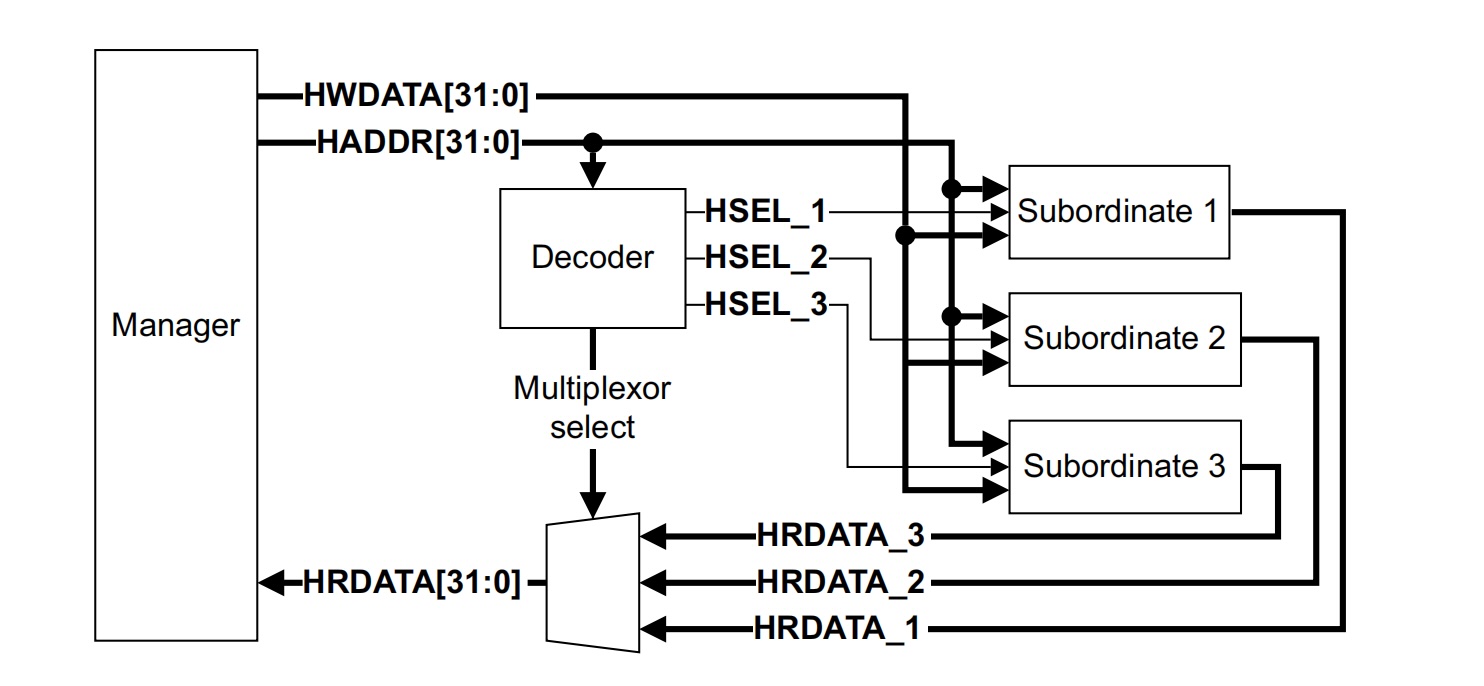
AHB Interconnection
Among the AHB slaves, the data memory (DMEM) is connected directly to the AHB bus as an AHB slave. All load/store instructions issued by the CPU are translated into AHB transactions through the LSU module, providing a straightforward path for data accesses.
All other low-bandwidth, register-mapped peripherals are accessed indirectly through an AHB-to-APB bridge, which itself appears as an AHB slave on the system bus. Behind this bridge, a set of APB peripherals is instantiated, including:
- GPIO
- SPI
- UART
- I²C
- Two general-purpose timers
The AHB-to-APB bridge decouples the higher-speed AHB domain from the simpler APB domain by:
- Translating AHB read/write transactions into APB transfers
- Generating APB select, enable, and write control signals for each peripheral
- Isolating the timing and fan-out of the peripheral bus from the main system bus
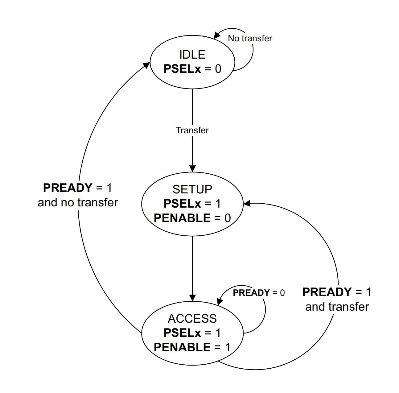
APB FSM Diagram
Peripherals
SPI
The first peripheral is SPI (Serial Peripheral Interface). SPI is a high-speed, full-duplex, synchronous serial communication protocol commonly used for data transmission between microcontrollers and peripherals. In our design, we use the open-source SPI from the PULP-Platform group to connect to the display.
UART
The second peripheral is UART (Universal Asynchronous Receiver/Transmitter). UART is an asynchronous serial communication protocol used for data transmission between devices. UART enables communication without a clock signal: the transmitter and receiver synchronize data transmission based on a predefined baud rate. It uses separate transmit (TX) and receive (RX) signals, allowing simultaneous data transmission and reception. The data format is start bit, data bits, optional parity bit, and stop bit.
GPIO
The third peripheral is GPIO (General-Purpose Input/Output). The GPIO module is designed to facilitate basic communication with external devices through eight GPIO pins. On the output path, each pin is controlled by a simple register that is updated whenever a write request is received from the bus. On the input path, a synchronizer composed of two back-to-back registers is implemented to prevent metastability. This ensures reliable input capture even under asynchronous conditions. When the processor issues a read request, the synchronizer's output value for the relevant pin is sent to the bus. This streamlined GPIO module balances simplicity and functionality, making it suitable for the proposed chip’s requirements.
I²C
The fourth peripheral is I²C (Inter-Integrated Circuit). Our design integrates an open-source I²C master controller to enable communication between devices using just two lines: SDA (data) and SCL (clock). The master handles operations like start, stop, read, and write while also monitoring bus status and managing multi-master arbitration. I²C offers efficient pin usage, the ability to support multiple peripherals through unique addresses, and compatibility with a wide range of low-speed devices such as sensors and EEPROMs.
Timer
The final peripherals are a pair of timers. The timer module is a versatile block designed to manage timing operations, generate events, and control pulse-width modulation (PWM). It supports both count-up and count-down modes and can operate with sawtooth or triangle-wave counting patterns. Timers synchronize events based on internal or external clock signals, making them suitable for various system control tasks such as delays, periodic interrupts, and signal generation. The timer configuration includes start and end counters, prescaler settings, and multiple compare channels. It generates interrupt or event signals upon matching the configured thresholds, enabling seamless integration into time-sensitive applications.
DFT Components
Scan Chain
The chip integrates a unified scan chain consisting of 248 scan cells, enabling full controllability and observability of key internal signals during DFT (Design-for-Test) and silicon bring-up. The scan chain forms a single linear shift register that spans modules including the instruction memory interface, data memory interface, clock generator, and the debug FSM.
The 248 scan cells connect a wide range of internal signals, including:
- IMEM signals: IMEM control, address, write enable, read and write data.
- DMEM signals: DMEM control, address, write enable, read and write data.
- Clock generator control signals.
- Debug FSM control and status signals.
These signals are flattened into a single contiguous scan path:

Scan Chain
This structure allows external test equipment or debugging software to shift in arbitrary patterns and read out internal states at any point.
Scan Mode Operation
In scan mode, the SoC suspends normal functional dataflow and all memory wrapper modules switch into test configuration:
- Functional read/write ports of IMEM and DMEM are disabled.
- Scan-in (SI) and scan-out (SO) signals propagate through the entire chain.
- All control signals connected to the scan chain are driven purely by the shifted scan data.
- The scan chain scans instructions into IMEM and data into DMEM for initialization.
- The scan chain can also read out the content of DMEM after program execution, enabling full post-silicon inspection of computation results.
Run Mode Operation
When scan mode is deactivated, the memory wrappers and control signals reconnect to their functional sources:
- The CPU fetches instructions directly from IMEM.
- The CPU accesses DMEM via the AHB bus.
- The clock generator operates according to the programmed settings.
- No scan traffic influences the functional logic.
The transition between scan mode and run mode is cleanly controlled to ensure no metastability or unintended corruption of memory or control registers.
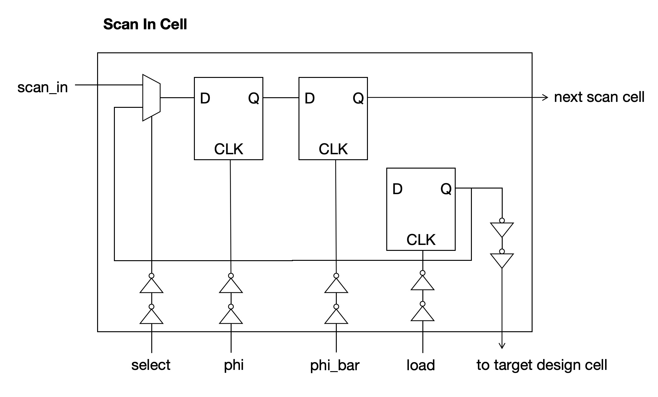
Scan In Cell
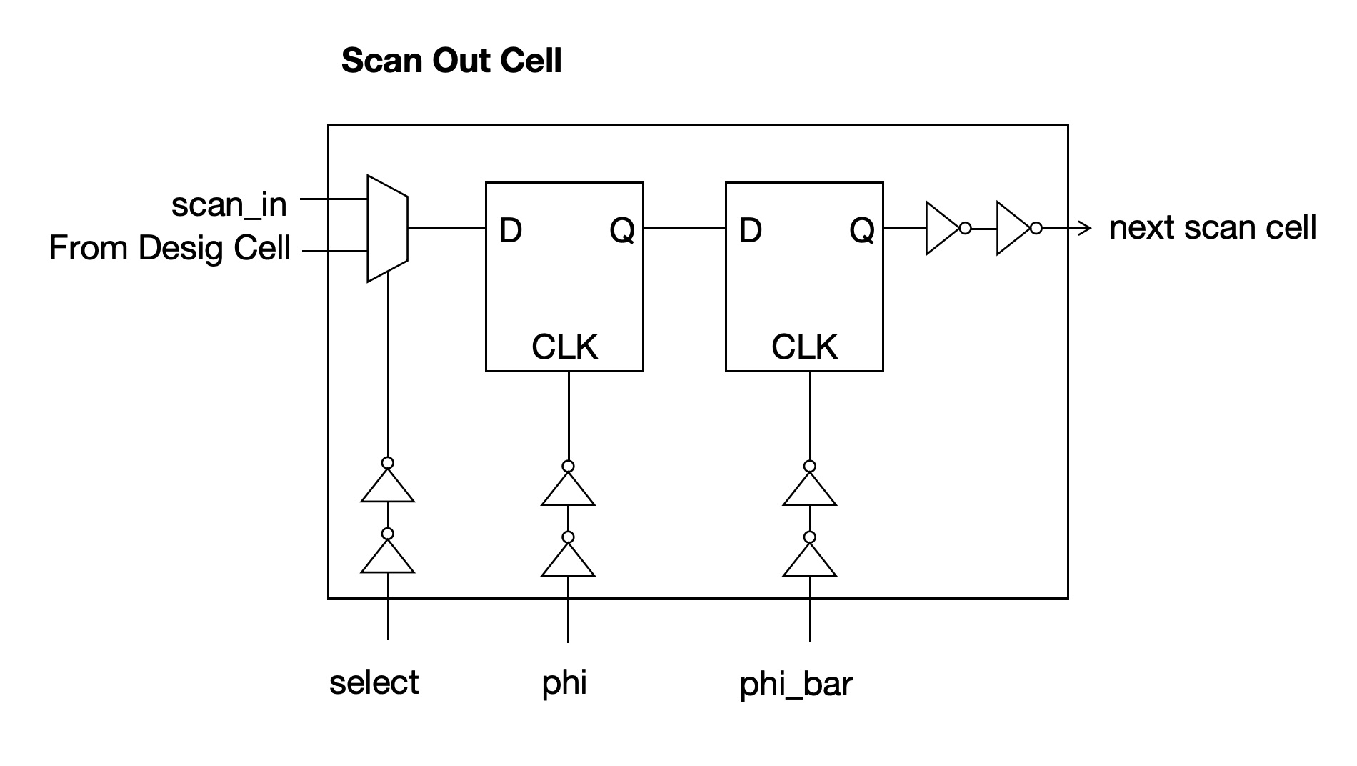
Scan Out Cell
Clock Generator
The clock generator is based on a ring oscillator whose output frequency can be configured at runtime through two control registers:
- fc (frequency control): selects the effective length of the ring oscillator, thereby adjusting the base oscillation frequency. Different fc settings correspond to different numbers of delay stages in the ring.
- div (divider): applies a programmable integer divide ratio to the ring oscillator output, generating a lower-frequency system clock when needed.
By combining the fc and div settings, the SoC can trade off performance, power consumption, and timing margin. These control bits are loaded via the scan chain, allowing the clock configuration to be changed even when no firmware is running yet. The final clock output of the generator is routed to the CPU core, AHB bus, memories, and peripherals, forming the primary system clock domain.
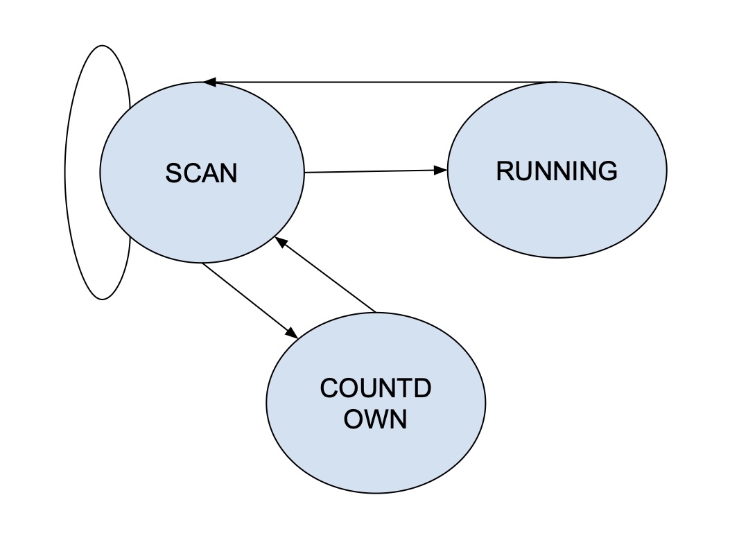
Debug FSM
A debug FSM orchestrates how the generated clock is delivered to the rest of the chip. The FSM supports three operating modes:
- Scan Mode: The system clock is not launched, and no clock edges are propagated to the CPU or peripherals. In this mode, the scan chain operates using the external scan clock; IMEM and DMEM clocks are driven by the scan clock.
- Run Mode: The clock generator output is continuously forwarded through the scan-controlled clock gating logic to the system clock tree. The SoC operates normally in this mode: the CPU executes instructions from IMEM, accesses DMEM over AHB, and interacts with APB peripherals.
- Debug Mode: The FSM enables the clock for a programmable number of cycles and then automatically returns to a paused state. This allows engineers to advance the system by a controlled number of clock edges and then inspect internal state or memory contents via the scan chain.
Mode selection, as well as auxiliary control signals (such as step length in debug mode), are loaded through the scan chain. This allows complete control of clock behavior from external test equipment without relying on software.
Debug FSM
Design Flow
This tape-out project follows a complete ASIC development flow that spans front-end design, back-end physical implementation, and post-silicon validation. The process begins with the system specification and microarchitecture design, where the functional requirements and architectural structure of the chip are defined. Based on this specification, the RTL is implemented in Verilog/SystemVerilog.
During the functional verification phase, both hardware testbenches and software programs are used. We developed a full RISC-V software toolchain and compiler to generate C-based test cases, allowing us to verify the CPU core using real workloads and instruction sequences. This hardware–software co-verification ensures correctness at both the microarchitectural and ISA levels before synthesis.
After verification, the RTL is synthesized into a gate-level netlist, followed by post-synthesis timing and functional checks. The design then enters the physical design flow, including floorplanning, power planning, placement, routing, and clock tree synthesis. I/O pad integration and layout optimization are performed prior to signoff verification, which includes STA, DRC, LVS, and ERC. Once the design passes all signoff checks, the final GDSII is generated and sent for tape-out.
Following fabrication, the bare dies are packaged and undergo bring-up on both a breadboard environment and a dedicated PCB. The entire PCB, including power regulation, signal breakouts, connectors, and measurement points, was fully designed by our team, with all components hand-selected to support chip evaluation. Silicon validation verifies real-chip functionality, performance, and power consumption. After successful validation, the chip is used for demonstrations and system-level experiments.
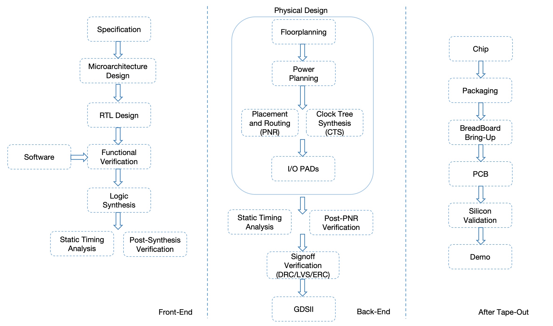
Chip Design Flow
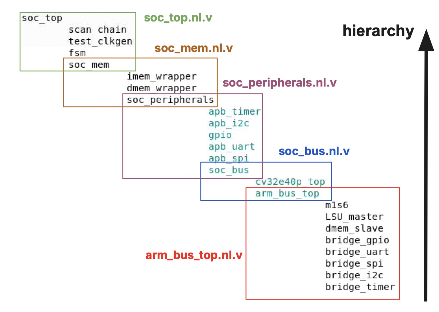
RTL Design
The RTL design of the SoC was developed and compiled using the ModelSim simulation environment. The codebase follows a clear hierarchical structure that separates chip-level integration, functional logic, and DFT infrastructure. At the highest level, the design begins with soc-pins, which connect the internal SoC signals to the padframe. Directly beneath it is soc-top, the actual top-level RTL of the chip. This module contains both the functional SoC and the DFT subsystem, which are designed as two independent power domains: the DFT logic operates under VDD_Test, while all functional logic is powered by VDD_Core. This separation ensures safe testing in scan mode without interfering with normal system behavior.
The functional portion of the chip is encapsulated in soc_mem, which contains the CPU core, memory subsystem, bus fabric, and peripheral subsystem. The CV32E40P RISC-V core connects directly to IMEM for instruction fetch, while DMEM access is performed through the AHB bus. Both memories are instantiated through custom wrappers that interface the synthesized RTL with the SRAM macros and support both run mode and scan mode. The same module instantiates the AHB interconnect, the AHB-to-APB bridge, and all APB peripherals, including UART, SPI, GPIO, I²C, and timers. This organization places all processor-visible functionality inside a single coherent RTL subsystem.
On the DFT side, soc-top integrates the full-chip scan chain, scan-mode clock control, and debug FSM, along with a separate test-mode clock generator netlist used for DFT simulations. The scan chain spans 248 cells and provides controllability and observability across CPU state, memory wrapper mode bits, the clock generator configuration registers, and peripheral-related scan points. This allows instructions and data to be shifted directly into IMEM and DMEM during bring-up, while also enabling cycle-stepping through the debug FSM.
Overall, the RTL is organized to cleanly separate functionality and test logic while maintaining a modular structure that mirrors the physical hierarchy of the final chip. This structure supported efficient simulation, synthesis, and later physical design, and provided a clear boundary between the functional SoC and its DFT infrastructure.
RTL Modules Architecture
Design Verification
The verification of the SoC followed a directed-test methodology using a custom SystemVerilog testbench together with C-based test programs compiled for the RISC-V architecture. Instead of building a full UVM environment, we adopted a focused, system-driven verification approach that closely matches the behavior of the real chip during board-level bring-up. This allowed us to validate both the functional design and the DFT infrastructure under realistic operating conditions.
All test cases were written as C programs, compiled using the RISC-V GCC toolchain, and executed directly on the embedded CV32E40P CPU core. These tests exercise the RTL in the same way real firmware will, enabling software-driven verification of processor execution, memory behavior, bus transactions, and peripheral functionality. A variety of targeted test programs were developed to isolate and validate individual modules—including DMEM read/write patterns, SPI transfers, UART transmission, GPIO toggling, I²C transactions, and timer interrupts. In addition to unit-level tests, we also created integrated programs that combine multiple peripherals and CPU-bus interactions to ensure correct end-to-end system behavior. More details of the test program structure and software toolchain will be described in the Software section.
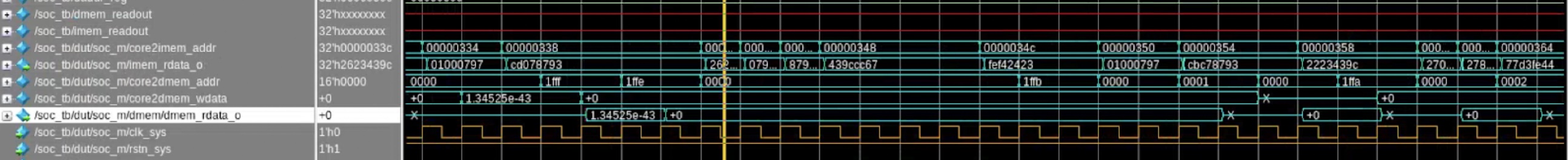
The SystemVerilog testbench models the full bring-up sequence of the physical chip. Before each run, the testbench assembles the 248-bit scan-in vector by organizing the scan chain fields according to their functional purposes, including IMEM contents, DMEM initialization, clock generator configuration, and FSM mode bits. Verification begins with a global reset, followed by placing the internal FSM into scan mode so that the testbench can shift instructions and configuration data into the scan chain. Once the scan load is complete, the FSM transitions into run mode, enabling the CPU to fetch instructions from IMEM and execute the compiled C program. Waveforms are monitored during execution to observe CPU behavior, AHB and APB transactions, peripheral activity, and memory accesses, ensuring architectural and protocol correctness.
After program execution finishes, the FSM is switched back into scan mode to shift out DMEM data. By comparing the scanned-out results against the expected outputs generated by the C test case, we verify the correctness of program execution, the integrity of the scan chain, and the functionality of the memory wrappers. This verification flow—reset → scan-in → run → scan-out—exactly mirrors the operational steps used during post-silicon bring-up, ensuring a high degree of consistency between pre-silicon simulation and hardware validation.
GPIO Write Test Case
GPIO Read and Memory Test Case
Post-Synthesis Reports
Synthesis
The synthesis stage translated the RTL design into a gate-level netlist using the TSMC 65 nm standard-cell library. Before synthesis, the RTL underwent linting and cleanup to ensure complete synthesizability and consistent signal definitions across modules. We constructed a comprehensive set of timing and design constraints, including the system clock specification, input and output delays, false-path and multicycle-path declarations, and mode-specific constraints for both functional and scan operation. These constraints ensured that the synthesis tool accurately captured the intended timing behavior of the SoC across all subsystems.
During synthesis, the memory wrappers were configured to replace their behavioral models with the actual SRAM hard macros generated by the memory compiler. The wrappers provided the necessary functional and scan-mode interfaces so that the macros could be seamlessly integrated into both the RTL and gate-level flows.
In our synthesis flow, we follow a hierarchical methodology aligned with the RTL file organization. All IP modules—such as the CPU core, SPI, UART, I²C, GPIO, timer, scan chain, and various FSMs—are synthesized individually to ensure modularity and ease of debugging. When synthesizing the SoC-level design, we include the previously generated netlists for these IP blocks and then proceed with synthesizing the SoC bus, SoC memory subsystem, and SoC top, together with the SRAM integration files.
For each test case, we perform post-synthesis gate-level simulation to validate functional correctness. Due to several modules exhibiting hold-time violations, not all test cases pass at this stage. These hold issues are expected and will be resolved during the physical design (PD) stage through proper buffering and timing refinement. Importantly, we ensure that there are no setup-time violations after synthesis, providing a solid timing foundation for the subsequent place-and-route process.
Following synthesis, we generated reports for area utilization, hierarchical timing, constraint coverage, and scan connectivity. The final synthesized netlist, along with the macro placement constraints and clock definitions, was handed off to the physical design stage for floorplanning and place-and-route. This marked the transition from RTL-level development to back-end implementation.
Timing and Area Summary
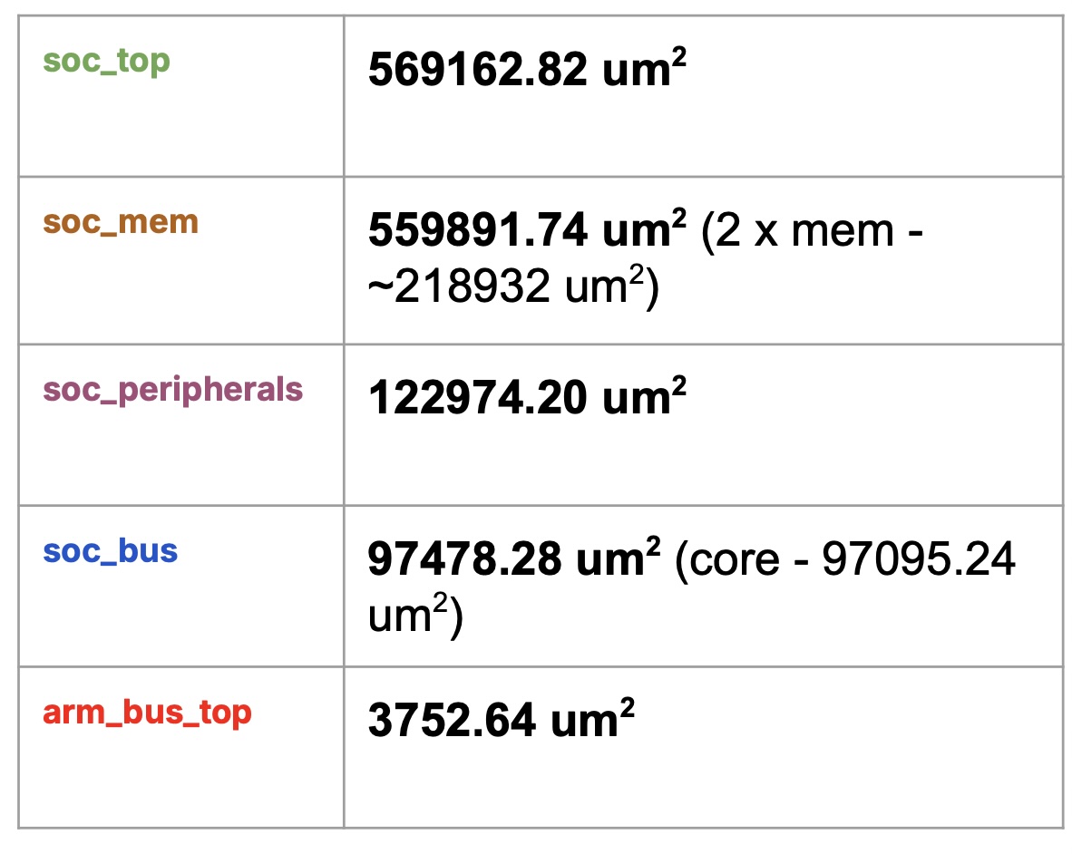
Gate-Level Results Overview
Physical Design
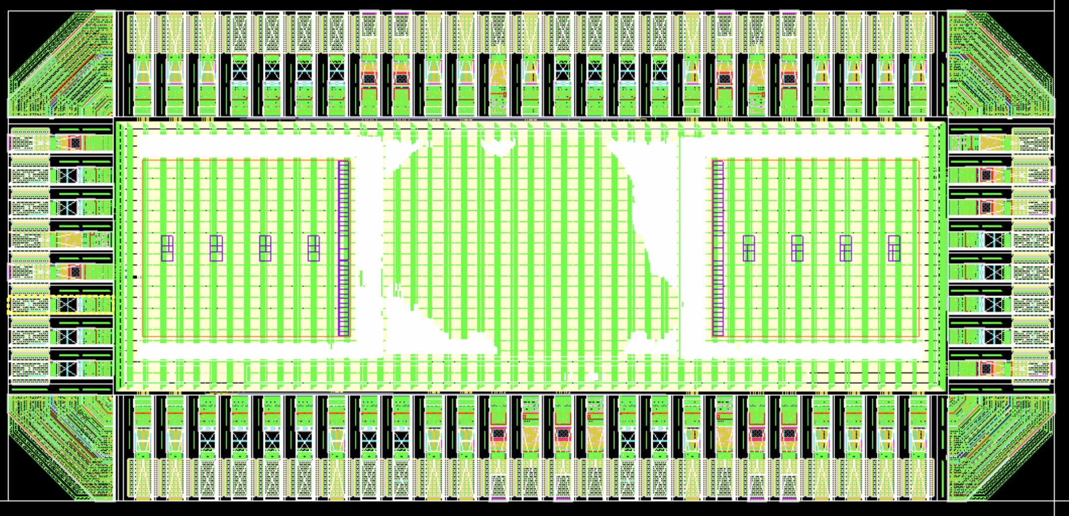
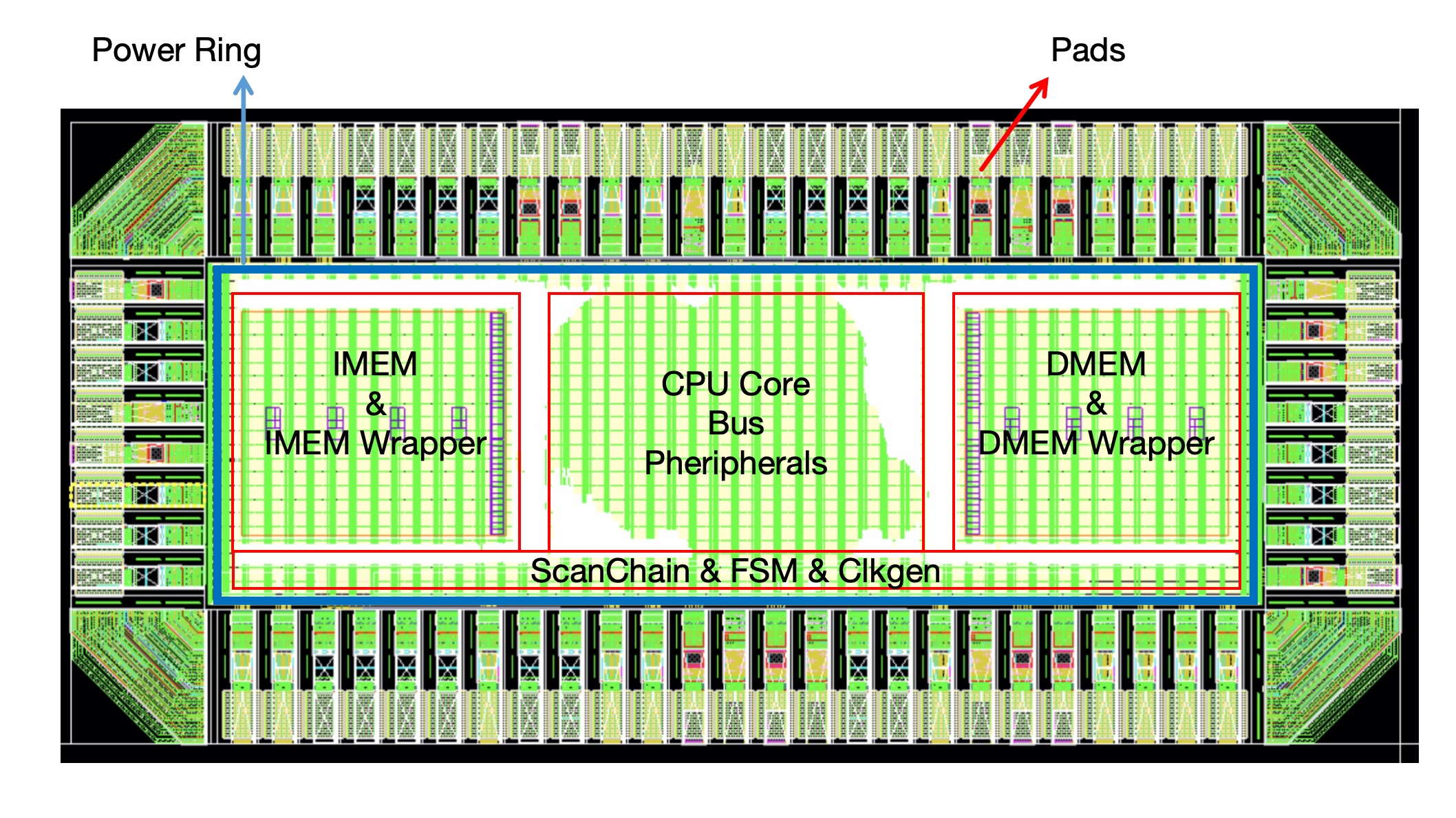
The physical design of the chip is implemented using Cadence Innovus for place-and-route and Cadence Virtuoso for final layout verification. We adopt a relatively simple but structured floorplan. The core complex, including the CPU core, system bus, and peripheral modules, is laid out as a single main block located at the center of the die. The instruction memory (IMEM) and data memory (DMEM) are implemented as two dedicated rectangular SRAM macros placed on the left and right sides of the core, respectively, to minimize critical-path interconnect length between the processor and the memories. The FSM, clock generation logic, and scan chain controller are grouped together and placed along one side of the chip. Since these blocks share the same power domain, this placement simplifies power distribution and also provides a clean topology for scan chain routing toward the rest of the design. IO pads are inserted along all four edges of the chip to interface the internal logic with the external environment and to close the power ring.
Our physical design flow in Innovus follows a standard industrial methodology. We begin by creating the floorplan, defining the core area and placing the major macros according to the architecture partition described above. Next, we generate the global and local power rails, ensuring robust power delivery to all modules in the single power domain. After that, we define and constrain all input and output ports, including timing constraints and IO placement guidelines. The standard-cell placement step is then performed, followed by pre-CTS (clock tree synthesis) optimization to reduce congestion, fix early timing issues, and improve design quality before building the clock tree.
We then perform clock tree synthesis to distribute the clock to all sequential elements while controlling skew and insertion delay. A round of post-CTS optimization is run to clean up timing violations that emerge after the clock network is inserted. Once the clocks and standard cells are in good shape, we proceed to signal routing, including global and detailed routing, to connect all nets while honoring design rules. After routing, we run extraction to generate accurate parasitic (RC) information and conduct further timing and design optimizations. At this stage, decoupling capacitors and filler cells are inserted as needed to maintain power integrity, close metal density requirements, and ensure manufacturability. Finally, the design goes through a series of verification steps within Innovus (such as basic DRC and timing checks), and the tape-out-ready layout and associated views are exported.
As mentioned earlier in the synthesis section, some modules exhibited hold-time violations at the netlist level. These issues are systematically resolved during the place-and-route stage. Using post-route parasitic information, we perform hold-fixing in Innovus by inserting delay cells and adjusting routing where necessary. Our goal is to eliminate all hold-time violations while preserving setup-time margins, so that the final implementation is both functionally correct and timing-clean under the target operating conditions.
After the place-and-route flow is completed, the final layout is imported into Cadence Virtuoso for signoff-level physical verification. We perform full-layout DRC (Design Rule Check) and LVS (Layout Versus Schematic) to ensure that the layout is free of rule violations and is electrically consistent with the synthesized netlist. In addition, we back-annotate the extracted delay information into our simulation environment and re-run the full set of test cases at the gate-level with timing. All test cases are verified to pass with correct waveforms and converged timing behavior, providing strong confidence in both functionality and implementation quality.
For timing signoff, we use Synopsys PrimeTime to perform static timing analysis across the relevant process, voltage, and temperature corners. Based on the extracted parasitics from the routed layout, we verify that no setup or hold violations remain on any timing path and that there are no additional issues such as excessive clock skew or unconstrained paths. Through this combination of Innovus PnR, Virtuoso physical verification, gate-level simulations with back-annotated delays, and PrimeTime static timing analysis, we ensure that the design is ready for fabrication with clean physical, functional, and timing signoff.

Core, Bus, and Peripherals Layout

Scan Chain Layout
In our physical design, the standard vertical power rails for each small module are implemented at metal layer M6, while the horizontal local power routing within the modules uses M1. Because the soc_mem block—which contains the CPU core, peripherals, and the two memory macros—also relies on vertically oriented power rails, its power grid must be precisely aligned with the internal module rails. Even a small offset would cause DRC violations due to misaligned straps or insufficient metal overlap. At the chip’s top level (soc_pin), the global power distribution network transitions to a higher metal layer, where wide horizontal power rails are used to provide low-resistance current delivery across the full SoC. This hierarchical alignment of vertical and horizontal power structures ensures correct connectivity, prevents DRC errors, and supports stable power distribution throughout the design.
Final Layout Views
Packaging Overview
The fabricated die has dimensions of 1000 µm × 2000 µm, and contains a total of 66 bond pads distributed symmetrically around the four sides of the chip. The pad arrangement consists of 25 pads on the north side, 25 pads on the south side, 8 pads on the west side, and 8 pads on the east side, providing full access to power rails, I/O interfaces, clocks, scan signals, and debug ports.
Each bond pad follows the standard TSMC 65 nm pad-frame specification. The nominal pad opening is 60 µm × 190 µm, or 30 µm × 190 µm when excluding the spacing region. This ensures compatibility with conventional gold wire bonding processes used in QFP and LQFP packaging flows.
A total of 20 dies will be packaged, with the primary package type selected as LQFP64L, which provides sufficient lead-out pins for all I/O and supply connections while maintaining a compact and low-cost footprint suitable for PCB mounting and system-level testing. The pad-to-pin mapping has been verified to comply with the 64-pin lead frame configuration.
Power and Ground Bonding
All VSS pads are highlighted in magenta in the bond diagram and are down-bonded directly to the exposed paddle, ensuring a low-impedance return path for the core and I/O grounds. This improves noise performance, reduces supply bounce during high-activity conditions, and provides robust ESD protection. The VDD rails are bonded individually to dedicated package pins to allow independent supply measurement and external regulation.
Bonding Diagram and Pinout
The bonding diagram shows the complete mapping between die pads and LQFP64L pins. Power, ground, GPIO, SPI, UART, scan chains, and test signals are organized to minimize crossing wires and to maintain short bond lengths. This arrangement improves manufacturability, reduces parasitic inductance, and enhances reliability.
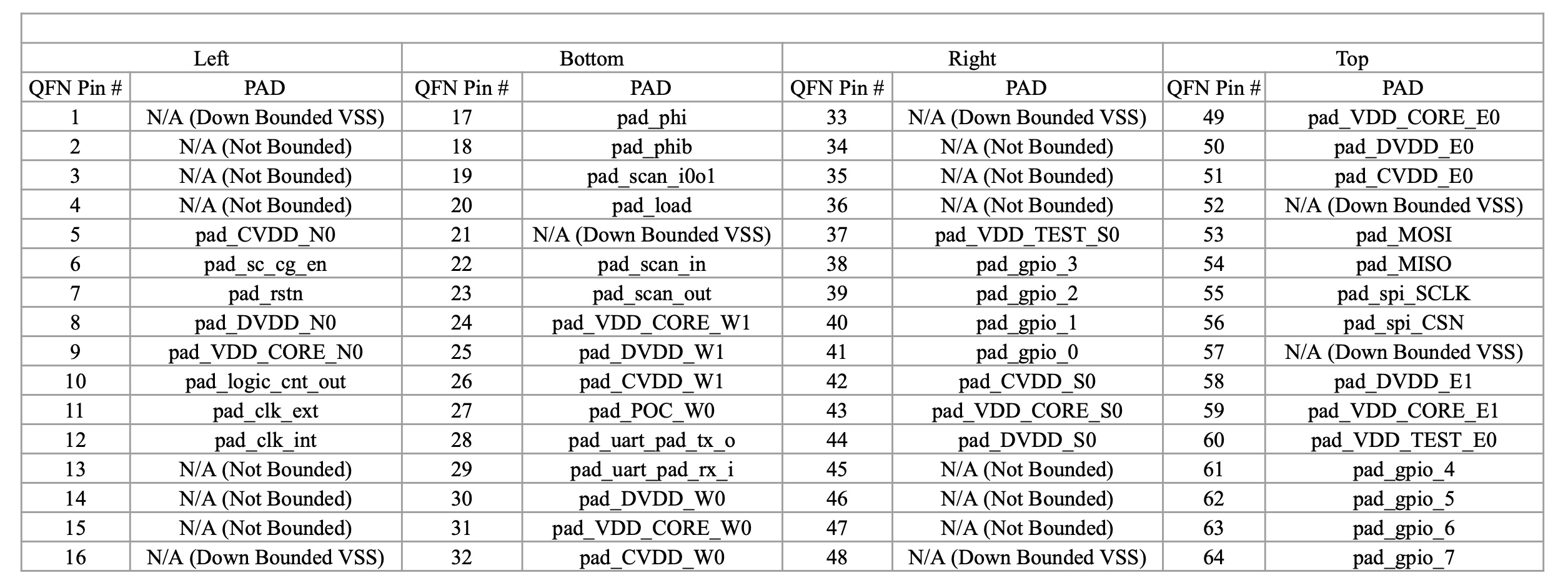
Bond Table
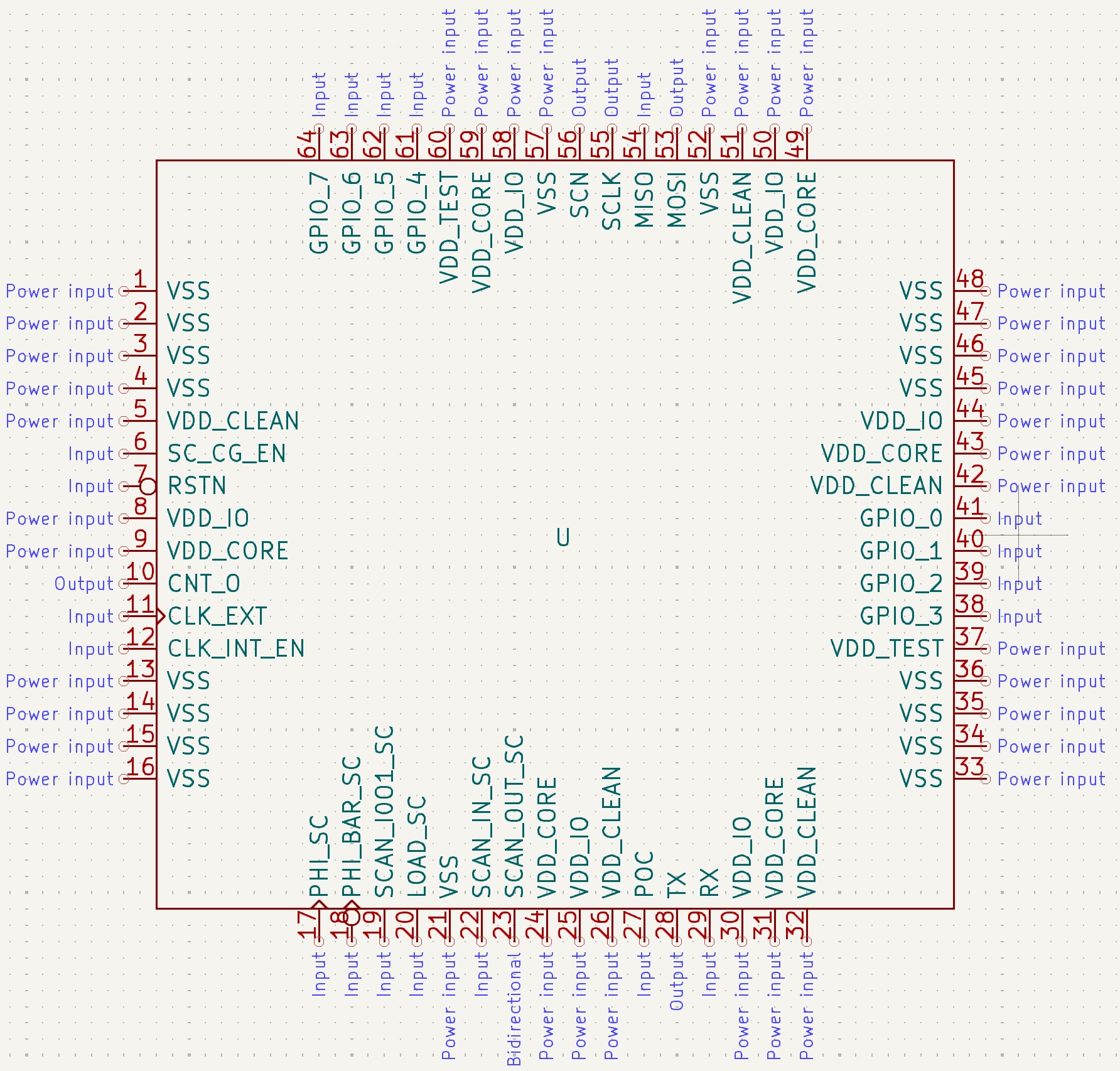
Bond Diagram
Software & Testing Flow
The software development and testing workflow begins with writing programs in C, which serve as test cases for validating the functionality of our SoC. To support this, we built a complete RISC-V toolchain, including a customized linker script and memory configuration. Since our design follows a Harvard architecture with separate instruction memory (IMEM) and data memory (DMEM), the toolchain is configured to correctly place code sections into IMEM and data sections into DMEM. The RISC-V compiler translates C programs into machine code, while also generating assembly output to assist with debugging and instruction-level verification. Once the C programs are compiled, the resulting machine code is loaded into the chip through the scan chain. During scan mode, the scan chain shifts the instructions directly into the IMEM and DMEM. After switching to run mode, the CPU begins fetching instructions from IMEM and executing them, allowing us to verify full-system behavior.
Custom linker script respects the Harvard split and AHB/APB address map.
Boot code, register aliases, and peripheral helpers reused across demos.
Generates IMEM/DMEM hex images for scan loading, simulation, and bring-up.
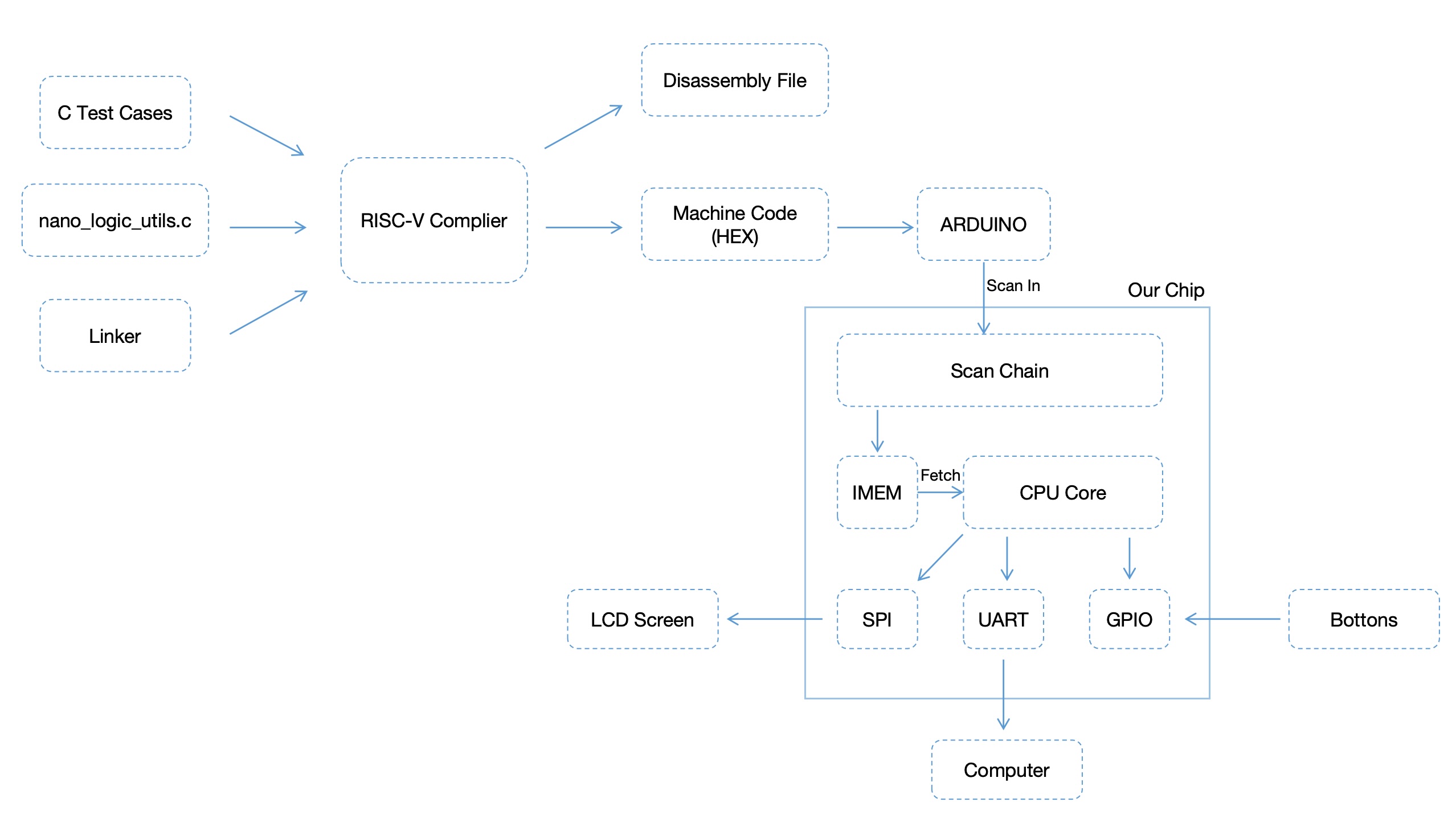
Chip Software Flow
Software Development
Compiler:
Our implementation of the CV32E40P core supports the RV32IMC instruction sets, and we built the corresponding RISC-V toolchain in order to compile C programs to run on our chip. We built the compiler before abandoning the FPU, so it also supports RV32Zfinx, which we simply don’t specify support for in our final bash script that calls the compiler.
Linker:
The linker is where things get a bit more complicated. GCC is designed for modified-Harvard and von-Neumann architectures, whereas our chip uses a pure Harvard Architecture. Our IMEM and DMEM both start at 0x0000_0000 and end at 0x0000_7FFF, which causes a perceived overlap between .text and .data in the linker. Our solution to this issue was to take advantage of the fact that we mask off the upper 16 bits of the word-aligned memory address coming out of the DMEM slave and into the DMEM wrapper.
As previously mentioned, in the DMEM slave, we shift the address right by 2 bits to ensure it is word-aligned. What was not mentioned is that we truncate the address on both sides, dropping both the lowest 2 bits, for word alignment, and the highest 14 bits, resulting in a 16-bit word-aligned address. A full 16-bit address was used as we designed the bus before finalising the size of our DMEM, and we wanted to leave wiggle room if we ended up having extra space. With our finalised 16KiB DMEM, we just ignore the top 4 bits of that address.
For our IO mapping, the AHB bus uses the most significant nibble of the 32-bit byte-aligned address coming from the CPU to determine the peripheral we want to talk to, so we need to keep that at 0 for DMEM. The second most significant nibble, however, is not used for routing and is masked off by the DMEM slave, so we set the second most significant nibble to 1, setting the origin of DMEM to 0x0100_0000 in the linker. The following example shows how it works:
Let's say that we want to write to address 0x4
The byte address is 0x00000004
The word address is 0x0000001
The final masked address is 0x00000001
But what if we wrote to address 0x01000004?
The byte address is 0x01000004
The word address is 0x00400001
The masked address is 0x00000001
Linker script (link.ld)
/* Copyright lowRISC contributors.
   Licensed under the Apache License, Version 2.0, see LICENSE for details.
   SPDX-License-Identifier: Apache-2.0 */

OUTPUT_ARCH(riscv)
MEMORY
{
    imem  : ORIGIN = 0x00000000, LENGTH = 0x4000          /* 32 kB */
    dmem  : ORIGIN = 0x01000000, LENGTH = 0x4000          /* 32 kB */
}

/* Stack information variables */
_min_stack     = 0x1000;   /* 4K - minimum stack space to reserve */
_stack_len     = LENGTH(dmem);
_stack_start   = ORIGIN(dmem) + LENGTH(dmem);

_entry_point = 0x0;
ENTRY(_entry_point)

SECTIONS
{
    .text : {
        . = ALIGN(4);
        *(.text)
        *(.text.*)
    }  > imem

    .rodata : {
        . = ALIGN(4);
        *(.rodata);
        *(.rodata.*)
    } > dmem

    .data : {
        . = ALIGN(4);
        *(.data);
        *(.data.*)
    } > dmem

    .bss :
    {
        . = ALIGN(4);
        _bss_start = .;
        *(.bss)
        *(.bss.*)
        *(COMMON)
        _bss_end = .;
    } > dmem

    /* ensure there is enough room for stack */
    .stack (NOLOAD): {
        . = ALIGN(4);
        . = . + _min_stack ;
        . = ALIGN(4);
        stack = . ;
        _stack = . ;
    } > dmem
}
Startup Handler:
With the compiler and linker set up, the next step was to create a startup routine that would reset the chip registers, point to the stack, and jump to the main function in the C program. This was done in assembly in crt0.S.
Startup routine (crt0.S)
# Copyright lowRISC contributors.
# Licensed under the Apache License, Version 2.0, see LICENSE for details.
# SPDX-License-Identifier: Apache-2.0

#define EXIT_SYSCALL 93

.section .text

reset_handler:
  /* set all registers to zero */
  mv  x1, x0
  mv  x2, x1
  mv  x3, x1
  mv  x4, x1
  mv  x5, x1
  mv  x6, x1
  mv  x7, x1
  mv  x8, x1
  mv  x9, x1
  mv x10, x1
  mv x11, x1
  mv x12, x1
  mv x13, x1
  mv x14, x1
  mv x15, x1
  mv x16, x1
  mv x17, x1
  mv x18, x1
  mv x19, x1
  mv x20, x1
  mv x21, x1
  mv x22, x1
  mv x23, x1
  mv x24, x1
  mv x25, x1
  mv x26, x1
  mv x27, x1
  mv x28, x1
  mv x29, x1
  mv x30, x1
  mv x31, x1

    /* stack initilization */
  la x2, _stack_start

_start:
  .global _start

  /* clear BSS */
  la x26, _bss_start
  la x27, _bss_end


main_entry:
  /* jump to main program entry point (argc = argv = 0) */
  addi x10, x0, 0
  addi x11, x0, 0
  jal x1, main

  /* If execution ends up here just put the core to sleep */
sleep_loop:
  wfi
  j sleep_loop
VHX Generator:
Ultimately, our programs need to end up as hexcode VHX files representing the raw data to load into IMEM and DMEM. To accomplish this, we have script, run.rv32.bash, which takes the specific C program, the linker, the startup routine, and any C files in our common folder, and compiles and links our C program. Once we have the object file, it is assembled into an ELF file, which is then disassembled into a DASM file and turned into our VHX files.
Build and VHX generation script
#!/bin/bash
clear

SRC_MAIN="src/demo/demo.c"

SRC_COMMON="common/crt0.S"
MAIN_BASE="$(basename -- ${SRC_MAIN})"
MAIN_NAME="${MAIN_BASE%.*}"
ELF="${MAIN_NAME%.*}.elf"
DASM="${MAIN_NAME%.*}.dasm"
VHX8="${MAIN_NAME%.*}.vhx8"
VHX32="${MAIN_NAME%.*}.vhx32"
VHX="${MAIN_NAME%.*}.vhx"

VHX8_INST="${MAIN_NAME%.*}_inst.vhx8"
VHX8_DATA="${MAIN_NAME%.*}_data.vhx8"
VHX32_INST="${MAIN_NAME%.*}_inst.vhx32"
VHX32_DATA="${MAIN_NAME%.*}_data.vhx32"
VHX_INST="${MAIN_NAME%.*}_inst.vhx"
VHX_DATA="${MAIN_NAME%.*}_data.vhx"

DIR_OBJ="obj"
DIR_ELF="elf"
DIR_DASM="dasm"
DIR_VHX="vhx"

PATH_BIN=" /tools/misc/CSEE4824/riscv_zfinx/bin"
CC="${PATH_BIN}/riscv32-unknown-elf-gcc"
LD="${CC}"
DUMP="${PATH_BIN}/riscv32-unknown-elf-objdump"
OBJCP="${PATH_BIN}/riscv32-unknown-elf-objcopy"
CFLAG="-march=rv32imc -mabi=ilp32 -static -mcmodel=medany -Wall -g -O0 -fvisibility=hidden -nostdlib -nostartfiles -ffreestanding "
INCS="-Icommon -Isrc"
LDFILE="common/link.ld"

rm -rf $DIR_OBJ/*

for DIR in $DIR_OBJ $DIR_DASM $DIR_ELF $DIR_VHX
do
mkdir -p $DIR
done

rm -f $DIR_ELF/$ELF
rm -f $DIR_DASM/$DASM
rm -f $DIR_VHX/$VHX8
rm -f $DIR_VHX/$VHX32


## OBJECT from SOURCE
for FSRC in ${SRC_COMMON} ${SRC_MAIN}
do
SRC_BASE="$(basename -- $FSRC)"
OBJ_NAME="${SRC_BASE%.*}"
OBJ="${OBJ_NAME}.o"
${CC} ${CFLAG} ${INCS} -MMD -c -o ${DIR_OBJ}/${OBJ} ${FSRC}
done

## OBJECT_LIST from OBJECT_FOLDER
LIST_OBJ=""
for OBJ_FILE in `ls ${DIR_OBJ}/*.o`
do
LIST_OBJ="${LIST_OBJ} ${OBJ_FILE}"
done

## ELF from OBJECT_LIST
${LD} ${CFLAG} ${INCS} -T ${LDFILE} -o ${DIR_ELF}/${ELF} ${LIST_OBJ}

## DISASSEMBLY from ELF
${DUMP} -fhSD ${DIR_ELF}/${ELF} > ${DIR_DASM}/${DASM}


## Verilog Hex from ELF
$OBJCP -O verilog ${DIR_ELF}/${ELF} ${DIR_VHX}/${VHX8}
$OBJCP -O verilog --only-section=.vectors  --only-section=.init --only-section=.text ${DIR_ELF}/${ELF} ${DIR_VHX}/${VHX8_INST}
$OBJCP -O verilog --only-section=.rodata --only-section=.data --only-section=.sdata --only-section=.bss --only-section=.stack ${DIR_ELF}/${ELF} ${DIR_VHX}/${VHX8_DATA}

python3 ./scripts/hex8tohex32.py ${DIR_VHX}/${VHX8} > ${DIR_VHX}/${VHX32}
python3 ./scripts/hex8tohex32.py ${DIR_VHX}/${VHX8_INST} > ${DIR_VHX}/${VHX32_INST}
python3 ./scripts/hex8tohex32.py ${DIR_VHX}/${VHX8_DATA} > ${DIR_VHX}/${VHX32_DATA}


grep -v '^@' ${DIR_VHX}/${VHX32} >  ${DIR_VHX}/${VHX}
grep -v '^@' ${DIR_VHX}/${VHX32_INST} >  ${DIR_VHX}/${VHX_INST}
grep -v '^@' ${DIR_VHX}/${VHX32_DATA} >  ${DIR_VHX}/${VHX_DATA}

printf "\n[DBG] Generated Files\n"
ls -lh ${DIR_ELF}/${ELF}
ls -lh ${DIR_VHX}/${VHX}
exit 1
Software Drivers:
There are two files which serve as software drivers for the IO on our chip, nano_logic_utils.c and spi_lcd_driver.h.
The main software driver is nano_logic_utils.c, which defines register mappings, initialization functions, and various other common functions for each of the peripherals. This driver is used in nearly all of our programs.
nano_logic_utils.c
/*
The file contains important definitions and functions to be used in writing programs
for our SoC.
*/

#include <stdint.h>
#include <stdio.h>
#include <stdlib.h>
#include <stdbool.h>

//Memory Location Definitions

//DMEM
#define DMEM_BASE 0x00000000 //Base address DMEM is mapped to

//GPIO
#define GPIO_BASE 0x10000000 //Base address GPIO is mapped to
#define GPIO_PADDIR 0x10000000 //Set direction of GPIO pins
#define GPIO_EN 0x10000004 //Enable input sampling on GPIO pins
#define GPIO_PADIN 0x10000008 //Read input signals from GPIO pins
#define GPIO_PADOUT 0x1000000C //Set output values of GPIO pins
#define GPIO_PADOUTSET 0x10000010 //Set output of GPIO pins high
#define GPIO_PADOUTCLR 0x10000014 //Set output of GPIO pins low
#define GPIO_INTEN 0x10000018 //Enable interrupts on GPIO pins
#define GPIO_INTTYPE 0x1000001C //Configure interrupt types for GPIO pins
#define GPIO_INTSTATUS 0x10000024
#define GPIO_PADCFG 0x10000028

//UART
#define UART_BASE 0x20000000 //Base address UART is mapped to
#define UART_LCR 0x2000000C //LCR is used for setting the Divisor Latch Access bit and the data format
#define UART_DLL 0x20000000 //DLL and DLM are used for setting the Baud Rate Divider value
#define UART_DLM 0x20000004 //DLL and DLM are used for setting the Baud Rate Divider value
#define UART_THR 0x20000000 //THR is used for Tx.
#define UART_RBR 0x20000000 //RBR is used for Rx.
#define UART_IER 0x20000004 //IER is set to interrupt the processor
#define UART_FCR 0x20000008 //FCR is used to clear the FIFO
#define UART_IIR 0x20000008 //IIR is used to identify interrupts
#define UART_MCR 0x20000010
#define UART_LSR 0x20000014
#define UART_MSR 0x20000018
#define UART_SCR 0x2000001C

//SPI
#define SPI_BASE 0x30000000 //Base address SPI is mapped to
#define SPI_STATUS 0x30000000
#define SPI_CLKDIV 0x30000004 //Clock divider value
#define SPI_CMD 0x30000008
#define SPI_ADR 0x3000000C
#define SPI_LEN 0x30000010 //Sets the length of DATA, ADDR, and CMD
#define SPI_DUM 0x30000014
#define SPI_TXFIFO 0x30000018 //FIFO storing value to transmit over MOSI
#define SPI_RXFIFO 0x30000020 //FIFO storing value received via MISO
#define SPI_INTCFG 0x30000024
#define SPI_INTSTA 0x30000028

//Timers
#define TIMER_BASE 0x50000000 //Base address the Timer Module is mapped to
#define TIMER_0_CNT 0x50000000 //Timer 0 count
#define TIMER_0_CTRL 0x50000004 //Timer 0 control
#define TIMER_0_CMP 0x50000008 //Timer 0 compare
#define TIMER_1_CNT 0x50000020 //Timer 1 count
#define TIMER_1_CTRL 0x50000024 //Timer 1 control
#define TIMER_1_CMP 0x50000028 //Timer 1 compare


//~~~~~~~~~~~~~~~~~~~~~~~~~~~~~~~~~~~~~~~~~~~~~
//Functions
//~~~~~~~~~~~~~~~~~~~~~~~~~~~~~~~~~~~~~~~~~~~~~


//Functions for Reading from and Writing to a Specific Address
#define ADDR_READ(addr) (*((volatile uint32_t *)(addr)))
#define ADDR_WRITE(addr, val) (*((volatile uint32_t *)(addr)) = val)


//---------------------------------------------
//GPIO Functions
//---------------------------------------------


// Note: Each GPIO instance occupies a 128-byte block (2^7 bytes).
// Full address = (instance number * 128) + local register offset.

//Used to initialize GPIO for transmission
void gpio_init() {

    // 1. Set all pins as inputs.
    ADDR_WRITE(GPIO_PADDIR, 0x00);

    // 2. Enable input sampling for pins.
    ADDR_WRITE(GPIO_EN, 0xff);

    // 3. Clear output values.
    ADDR_WRITE(GPIO_PADOUT, 0x00);

    // Optionally, clear any pending output set/clear signals.
    ADDR_WRITE(GPIO_PADOUTCLR, 0xff);  // Clear any outputs
    ADDR_WRITE(GPIO_PADOUTSET, 0x00);  // Ensure no outputs are forced high

    // 4. Disable interrupts.
    // Write 0 to disable all GPIO interrupts.
    ADDR_WRITE(GPIO_INTEN, 0x00);

    // 5. Set interrupt type to a default value.
    // Here, 0x00000000 might correspond to a default (e.g., falling-edge or disabled)
    ADDR_WRITE(GPIO_INTTYPE, 0x00);

    // 6. Set pad configuration to default.
    ADDR_WRITE(GPIO_PADCFG, 0x00);
}


/*
Set the direction of a single GPIO pin.
'pin_num' selects the pin (only lower 3 bits are used, as there are 8 pins).
'out' is true for output, false for input.
*/
static inline void gpio_set_pin_dir(uint32_t out) {
    ADDR_WRITE(GPIO_PADDIR, out);
    ADDR_WRITE(GPIO_EN, ~out); //Do we need this line if we set them all to be able to sample in the initialization function?
}

/*
Write a boolean value to a single GPIO pin.
'data' true sets the pin high; false clears the pin.
*/
static inline void gpio_pin_write(uint32_t data) {
    ADDR_WRITE(GPIO_PADOUT, data);
}

/*
Read the value from a single GPIO pin.
Returns true if the pin is high, false if low.
*/
static inline uint32_t gpio_pin_read() {
    return ADDR_READ(GPIO_PADIN);
}


//---------------------------------------------
//UART Functions
//---------------------------------------------


//Used to initialize UART for byte-wise transmission.
void uart_init() {

    ADDR_WRITE(UART_LCR, 0x00000081);

    ADDR_WRITE(UART_DLL, 0x00000059);
    ADDR_WRITE(UART_DLM, 0x00000022);
    //Baud rate of 9600 for 84.414MHz clock speed. (Baud rate = clk_freq/DLM:DLL)

    //Sending one byte at a time
    ADDR_WRITE(UART_LCR, 0x00000003);
    ADDR_WRITE(UART_THR, 0x0000000A);
	ADDR_WRITE(UART_THR, 0x0000000A);
	ADDR_WRITE(UART_THR, 0x0000000A);
	ADDR_WRITE(UART_THR, 0x0000000A);
	ADDR_WRITE(UART_THR, 0x0000000A);
	ADDR_WRITE(UART_THR, 0x0000000A);
}

/*
Used to transmit a byte over UART, note that the byte is transmitted LSB first.

Takes an 8-bit value data which is the byte to be transmitted
*/
static inline void uart_transmit_char(uint8_t data) {
    ADDR_WRITE(UART_THR, data);
}

//---------------------------------------------
//SPI Functions
//---------------------------------------------

//Used to initialize SPI for transmission
void spi_init(){
    //Setting length of DATA, ADDR, CMD to one byte each
    ADDR_WRITE(SPI_LEN, 0x00080808);

    ADDR_WRITE(SPI_CLKDIV, 0x000000FF);
}

/*
Used to transmit a packet over SPI

Takes a 1-byte command, 1-byte address, and 1-byte data value to be transmitted over SPI
*/
static inline void spi_transmit(uint8_t cmd, uint8_t adr, uint8_t data){
    ADDR_WRITE(SPI_CMD, cmd << 24);
    ADDR_WRITE(SPI_ADR, adr << 24);
    ADDR_WRITE(SPI_TXFIFO, data << 24);
    ADDR_WRITE(SPI_STATUS, 0x00000102);
}

//---------------------------------------------
//Timer Functions
//---------------------------------------------

/*
Used to (re)start the count of the specified timer from 0.

Takes in a bool timer which specifies which timer, 0 or 1,
should be (re)started
*/
void timer_reset_and_start(bool timer) {
    if (timer) {

        //Reset timer 1 count to 0
        ADDR_WRITE(TIMER_1_CNT, 0x00000000);

        //Enable timer 1
        ADDR_WRITE(TIMER_1_CTRL, 0x00000019);
    }
    else {
        //Reset timer 0 count to 0
        ADDR_WRITE(TIMER_0_CNT, 0x00000000);

        //Enable timer 0
        ADDR_WRITE(TIMER_0_CTRL, 0x00000019);
    }
}

/*
Used to read the current count value of the specified timer.

Takes in a bool timer which specifies which timer, 0 or 1,
should be read
*/
static inline uint32_t timer_read(bool timer) {
    if (timer) return ADDR_READ(TIMER_1_CNT);
    else return ADDR_READ(TIMER_0_CNT);
}

/*
void timer_set_compare(bool timer, uint32_t comp) {
    if (timer) ADDR_WRITE(TIMER_1_CMP, comp);
    else ADDR_WRITE(TIMER_0_CMP, comp);
}
*/


//---------------------------------------------
//Delay Functions
//---------------------------------------------
static inline void delay(int n) {
    // Simple delay loop (adjust based on your system clock)
    volatile int i;
    for (i = 0; i < n * 100; i++) {}
}

// ------------ UART helpers (single-char only) ------------
  static void uart_putc(char c) {
      uart_transmit_char((uint8_t)c);
  }
The other software driver, spi_lcd_driver.h, is responsible for defining functions to control the SPI LCD backpack. This code is based on a previous group's driver for the same backpack [4]
spi_lcd_driver.h
// Code based on spi_lcd.h from https://gitfront.io/r/lafis002/nsQYcfC2svzE/iRisc/

#include "nano_logic_utils.c"

#define HIGH 1
#define LOW 0

volatile uint32_t SPIbuff;
volatile uint8_t  displaycontrol;

void long_delay(int n) {
	volatile int i;
	for (i = 0; i < n * 1000; i++) {}
}

void spi_write(volatile uint32_t cmd, volatile uint8_t DELAY){
	ADDR_WRITE(SPI_CMD, cmd); //8 bits of CMD we want to send to LCD
	ADDR_WRITE(SPI_ADR, cmd); //8 bits of ADDR we want to send to LCD
	ADDR_WRITE(SPI_TXFIFO, cmd);
	ADDR_WRITE(SPI_STATUS, 0x00000102); //Enable the clk to peripheral (SPI clk). Bit [1] set to enable spi_wr mode, and bit [8] set to chip select LCD.
	long_delay(DELAY);
}


void lcd_init(volatile uint8_t DELAY) {


	ADDR_WRITE(SPI_LEN, 0x00080808); //Setting length of DATA, ADDR, CMD
	ADDR_WRITE(SPI_CLKDIV, 0x000000FF); //Setting clock divider factor

	spi_write(0x80000000, DELAY); //_digitalWrite(_rs_pin, LOW); Line 188, Adafruit_LiquidCrystal.cpp
	spi_write(0x80000000, DELAY); //_digitalWrite(_enable_pin, LOW); Line 189, Adafruit_LiquidCrystal.cpp


	//write4bits(0x03); Line 200, Adafruit_LiquidCrystal.cpp
	spi_write(0xC0000000, DELAY);
	spi_write(0xE0000000, DELAY);
	spi_write(0xE0000000, DELAY);
	spi_write(0xE0000000, DELAY);
	spi_write(0xE0000000, DELAY);
	spi_write(0xE4000000, DELAY);
	spi_write(0xE0000000, DELAY);

	//delayMicroseconds(4500); Line 201, Adafruit_LiquidCrystal.cpp
	long_delay(100);

	//write4bits(0x03); Line 204, Adafruit_LiquidCrystal.cpp
	spi_write(0xE0000000, DELAY);
	spi_write(0xE0000000, DELAY);
	spi_write(0xE0000000, DELAY);
	spi_write(0xE0000000, DELAY);
	spi_write(0xE0000000, DELAY);
	spi_write(0xE4000000, DELAY);
	spi_write(0xE0000000, DELAY);

	//delayMicroseconds(4500); Line 205, Adafruit_LiquidCrystal.cpp
	long_delay(100);

	//write4bits(0x03); Line 208, Adafruit_LiquidCrystal.cpp
	spi_write(0xE0000000, DELAY);
	spi_write(0xE0000000, DELAY);
	spi_write(0xE0000000, DELAY);
	spi_write(0xE0000000, DELAY);
	spi_write(0xE0000000, DELAY);
	spi_write(0xE4000000, DELAY);
	spi_write(0xE0000000, DELAY);

	//delayMicroseconds(150); Line 209. Delay given below (1000) is more than required, can be changed
	long_delay(1000);

	//write4bits(0x02); Line 212, Adafruit_LiquidCrystal.cpp
	spi_write(0xA0000000, DELAY);
	spi_write(0xA0000000, DELAY);
	spi_write(0xA0000000, DELAY);
	spi_write(0xA0000000, DELAY);
	spi_write(0xA0000000, DELAY);
	spi_write(0xA4000000, DELAY);
	spi_write(0xA0000000, DELAY);

	long_delay(100); //Needed???

	//command(LCD_FUNCTIONSET | _displayfunction); Line 230, Adafruit_LiquidCrystal.cpp
	//LCD_FUNCTIONSET | _displayfunction evalutaes to 0x28
	spi_write(0xA0000000, DELAY); //_digitalWrite(_rs_pin, mode); Line 401, Adafruit_LiquidCrystal.cpp
	spi_write(0xA0000000, DELAY);
	spi_write(0xA0000000, DELAY);
	spi_write(0xA0000000, DELAY);
	spi_write(0xA0000000, DELAY);
	spi_write(0xA0000000, DELAY);
	spi_write(0xA4000000, DELAY);
	spi_write(0xA0000000, DELAY);

	spi_write(0xA0000000, DELAY);
	spi_write(0x80000000, DELAY);
	spi_write(0x80000000, DELAY);
	spi_write(0x88000000, DELAY);
	spi_write(0x88000000, DELAY);
	spi_write(0x8C000000, DELAY);
	spi_write(0x88000000, DELAY);

	//display(); Line 234, Adafruit_LiquidCrystal.cpp
	spi_write(0x88000000, DELAY); //_digitalWrite(_rs_pin, mode); Line 401, Adafruit_LiquidCrystal.cpp

	spi_write(0x88000000, DELAY);
	spi_write(0x88000000, DELAY);
	spi_write(0x88000000, DELAY);
	spi_write(0x80000000, DELAY);
	spi_write(0x80000000, DELAY);
	spi_write(0x84000000, DELAY);
	spi_write(0x80000000, DELAY);

	spi_write(0x80000000, DELAY);
	spi_write(0x80000000, DELAY);
	spi_write(0x90000000, DELAY);
	spi_write(0x98000000, DELAY);
	spi_write(0x98000000, DELAY);
	spi_write(0x9C000000, DELAY);
	spi_write(0x98000000, DELAY);

	//clear(); Line 237, Adafruit_LiquidCrystal.cpp
	spi_write(0x98000000, DELAY); //_digitalWrite(_rs_pin, mode); Line 401, Adafruit_LiquidCrystal.cpp
	spi_write(0x98000000, DELAY);
	spi_write(0x98000000, DELAY);
	spi_write(0x88000000, DELAY);
	spi_write(0x80000000, DELAY);
	spi_write(0x80000000, DELAY);
	spi_write(0x84000000, DELAY);
	spi_write(0x80000000, DELAY);

	spi_write(0xC0000000, DELAY);
	spi_write(0xC0000000, DELAY);
	spi_write(0xC0000000, DELAY);
	spi_write(0xC0000000, DELAY);
	spi_write(0xC0000000, DELAY);
	spi_write(0xC4000000, DELAY);
	spi_write(0xC0000000, DELAY);

	long_delay(100); //delayMicroseconds(2000); Line 250, Adafruit_LiquidCrystal.cpp

	//command(LCD_ENTRYMODESET | _displaymode); Line 242, Adafruit_LiquidCrystal.cpp
	spi_write(0xC0000000, DELAY); //_digitalWrite(_rs_pin, mode); Line 401, Adafruit_LiquidCrystal.cpp
	spi_write(0x80000000, DELAY);
	spi_write(0x80000000, DELAY);
	spi_write(0x80000000, DELAY);
	spi_write(0x80000000, DELAY);
	spi_write(0x80000000, DELAY);
	spi_write(0x84000000, DELAY);
	spi_write(0x80000000, DELAY);

	spi_write(0x80000000, DELAY);
	spi_write(0xA0000000, DELAY);
	spi_write(0xB0000000, DELAY);
	spi_write(0xB0000000, DELAY);
	spi_write(0xB0000000, DELAY);
	spi_write(0xB4000000, DELAY);
	spi_write(0xB0000000, DELAY);

	SPIbuff = 0x000000B0;
	displaycontrol = 0x04;
}

void digitalWrite(volatile uint8_t p, volatile uint8_t d, volatile uint8_t DELAY) {

	volatile uint32_t mask = 0xFF000000;

	if (d == HIGH)
		SPIbuff |= (1 << p);
	else
		SPIbuff &= ~(1 << p);

	volatile uint32_t word = mask &  (SPIbuff << 24);
	spi_write(word, DELAY);

}


void lcd_write(volatile uint8_t character, volatile uint8_t mode, volatile uint8_t DELAY) {
	// Implementing "send" function

	digitalWrite((uint8_t) 1, mode, DELAY);

	digitalWrite((uint8_t) 6, (uint8_t) ((character >> 4) & 0x01), DELAY);
	digitalWrite((uint8_t) 5, (uint8_t) ((character >> 5) & 0x01), DELAY);
	digitalWrite((uint8_t) 4, (uint8_t) ((character >> 6) & 0x01), DELAY);
	digitalWrite((uint8_t) 3, (uint8_t) ((character >> 7) & 0x01), DELAY);

	digitalWrite((uint8_t) 2, (uint8_t) LOW, DELAY);
	digitalWrite((uint8_t) 2, (uint8_t) HIGH, DELAY);
	digitalWrite((uint8_t) 2, (uint8_t) LOW, DELAY);


	digitalWrite((uint8_t) 6, (uint8_t) ((character >> 0) & 0x01), DELAY);
	digitalWrite((uint8_t) 5, (uint8_t) ((character >> 1) & 0x01), DELAY);
	digitalWrite((uint8_t) 4, (uint8_t) ((character >> 2) & 0x01), DELAY);
	digitalWrite((uint8_t) 3, (uint8_t) ((character >> 3) & 0x01), DELAY);

	digitalWrite((uint8_t) 2, (uint8_t) LOW, DELAY);
	digitalWrite((uint8_t) 2, (uint8_t) HIGH, DELAY);
	digitalWrite((uint8_t) 2, (uint8_t) LOW, DELAY);

}

void lcd_print(volatile char *string, volatile uint8_t size, volatile uint8_t DELAY) {

	volatile int i = 0;
	//uart_putc('S');
	//uart_putc('T');
	//uart_putc('R');
	//uart_putc(':');
	//uart_putc(' ');

	while (i < size) {
		lcd_write((uint8_t) string[i], (uint8_t) HIGH, DELAY);
		//uart_putc((uint8_t) string[i]);
		i++;
	}
		//uart_putc('\n');

}


void clear() {

	lcd_write((uint8_t) 0x01, (uint8_t) LOW, 1);
	long_delay(100);
}

void home() {


	lcd_write((uint8_t) 0x02, (uint8_t) LOW, 1);
	long_delay(100);
}

void setCursor(volatile uint8_t col, volatile uint8_t row, volatile uint8_t DELAY) {


	if (row == 0)
  		lcd_write((uint8_t) (0x80 | (col + 0x00)), (uint8_t) LOW, DELAY);
	else if (row == 1)
		lcd_write((uint8_t) (0x80 | (col + 0x40)), (uint8_t) LOW, DELAY);
	else if (row == 2)
		lcd_write((uint8_t) (0x80 | (col + 0x14)), (uint8_t) LOW, DELAY);
	else
		lcd_write((uint8_t) (0x80 | (col + 0x54)), (uint8_t) LOW, DELAY);

}

void noDisplay() {

	displaycontrol = 0x00;
	lcd_write((uint8_t) 0x08, (uint8_t) LOW, 1);

}

void display() {

	displaycontrol = 0x04;
	lcd_write((uint8_t) 0x0C, (uint8_t) LOW, 1);

}

void noCursor() {

	displaycontrol &= ~(0x02);

	lcd_write((uint8_t) (0x08 | displaycontrol), (uint8_t) LOW, 1);

}

void cursor() {

	displaycontrol |= 0x02;
	lcd_write((uint8_t) (0x08 | displaycontrol), (uint8_t) LOW, 1);

}

void noBlink() {

	displaycontrol &= ~(0x01);
	lcd_write((uint8_t) (0x08 | displaycontrol), (uint8_t) LOW, 1);

}

void blink() {

	displaycontrol |= 0x01;
	lcd_write((uint8_t) (0x08 | displaycontrol), (uint8_t) LOW, 1);

}

void scrollDisplayLeft() {

	lcd_write((uint8_t) 0x18, (uint8_t) LOW, 1);

}

void scrollDisplayRight() {

	lcd_write((uint8_t) 0x1C, (uint8_t) LOW, 1);

}

void setBacklight (uint8_t value) {

	digitalWrite((uint8_t) 0x07, value, 1);
}
Full demo program sources now live in the Demonstration section below.
Testing Methodology
Post-Silicon Validation
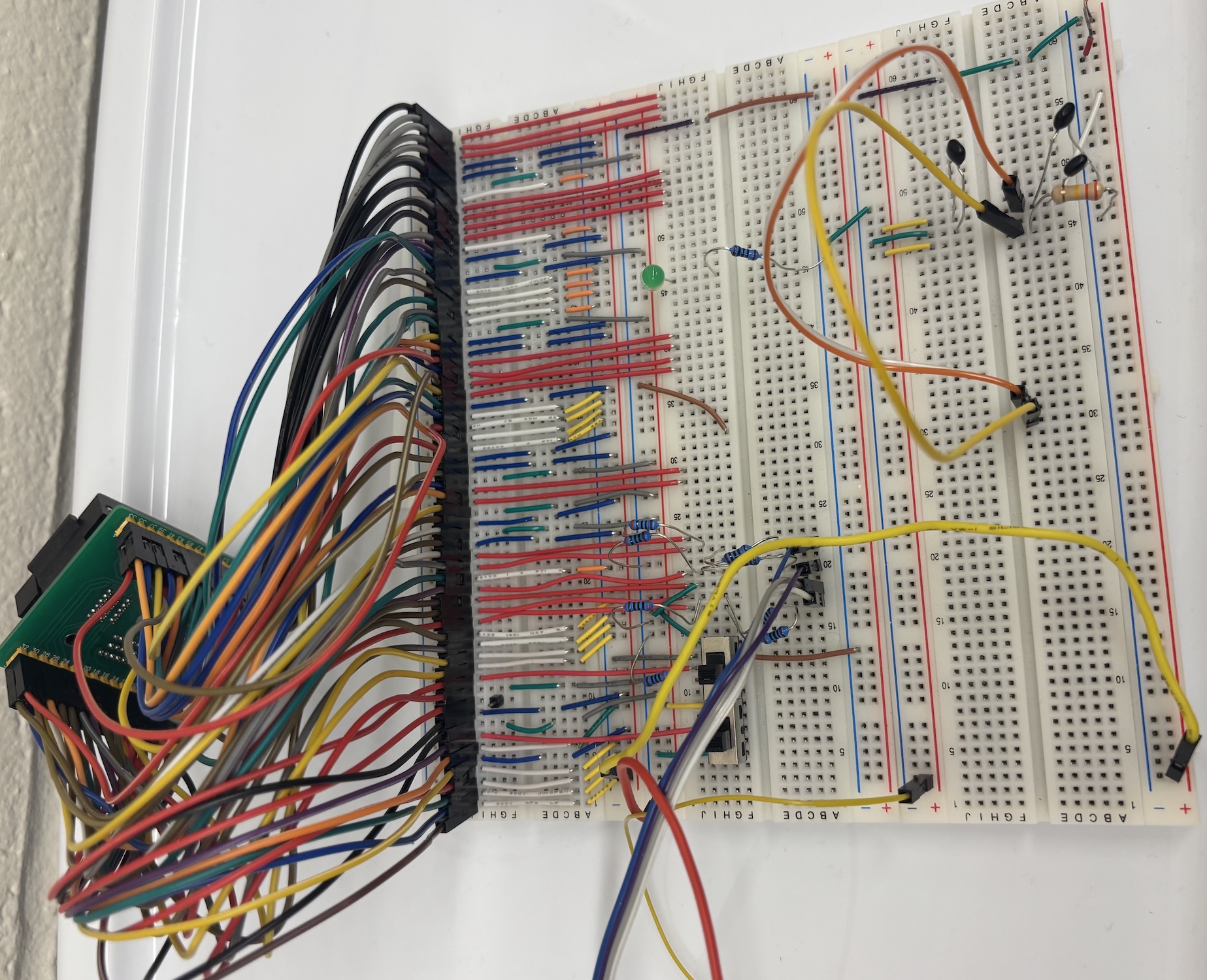
To conduct post-silicon validation on our chip, we started with a structured bring-up sequence to validate that the silicon was healthy. The very first step was to construct a testing setup on a breadboard that would allow us to test the various features of our chip. To make the setup easier, we used a QFP64 socket, which allowed us to connect our chip to the breadboard without soldering. Since the chip has 64 pins, and a single breadboard has 63 rows, each row of the breadboard was connected to pins 1 through 63 on the chip. Pin 64, which is GPIO 7, was left disconnected since there was no room, and it wasn't crucial for initial testing anyway. From there, the breadboard was set up in such a way as to mimic our testbench used in simulation. Specifically, we were most concerned with replicating the scan-chain process.
To do this, we first documented the expected values and behavior of each pin based on the simulation testbench. This included identifying which pins needed to be set to what voltage, which served as scan-chain controls, which were dedicated I/O pins, and which supplied power or clocking. Having this reference made it possible to map physical pin behavior to the functional waveforms we expected to observe on the oscilloscope.
Our initial plan was to use a 3.3 V Arduino Pro Mini as the external controller for scan-chain operations and general chip bring-up. However, we quickly discovered that the Pro Mini's microcontroller was not compatible with the routines in our scan-chain driver code. As a result, we switched to a 5 V Arduino Uno, using a voltage divider network to ensure that any 5 V outputs feeding into our chip were stepped down to safe levels. This let us continue development while maintaining signal integrity and protecting the silicon.
Once the control hardware was selected, we programmed the Arduino with a scan-chain interface based on code from a previous project in the course. This gave us an immediate framework for clocking in scan data, latching instructions, and reading chain outputs. With this basic infrastructure ready, we attached an oscilloscope to measure the internal clock generator. Our goal was to verify that the on-chip oscillator was functional and running at the intended frequency. After several measurement attempts, including adjusting trigger levels and confirming that our power rails were stable, we were able to confirm oscillation.
With the core clock verified, we moved on to testing individual subsystems. UART was the first to come online. After configuring baud rate parameters and validating the UART TX waveforms on the oscilloscope, we successfully received UART messages from the chip. This allowed us to use UART as a lightweight diagnostic channel for subsequent tests.
Next, we tested GPIO inputs. By manually toggling input pins and reading the chip's internal state over UART, we confirmed that the GPIO block was latching external values correctly. This validated both the input pads and the internal routing to the processor core.
For SPI testing, we created a test program to control the SPI pins and verified via oscilloscope that the chip generated the correct clock and data responses. Although initially noisy, after adjusting grounding on the breadboard and shortening several long wires, the SPI signals became reliable.
One of the more complex peripherals to bring up was the LCD SPI backpack interface. With SPI known working, and using the previous project's LCD SPI backpack driver as a foundation, we adapted the initialization and command routines to work with our chip's instruction format and GPIO mapping. This took several rounds of debugging, but ultimately the LCD displayed correct characters, confirming functional integration between GPIO, instruction memory, and the CPU datapath.
As we became more confident in the system's stability, we returned to improving our scan-chain infrastructure. The initial version loaded all scan data into a unified chain, but for full testing flexibility, we modified the code to load instruction memory and data memory independently. This allowed us to preload programs while separately initializing memory contents used for testing. It also fixed the remaining bug we had with the LCD, where it would often display garbage data, since the string data was not being properly loaded into data memory.
With the breadboard prototype functioning well, we began transitioning toward a standalone PCB. First, we replaced the variable-voltage bench supply with a dedicated 5 V-to-1 V regulator circuit, ensuring a stable and repeatable power configuration. Then, using lessons learned from the breadboard setup, we created the first revision of the PCB. This initial design focused on routing clarity and ensuring all chip pins were accessible for test points. Once fabricated, we tested this board thoroughly, checking power distribution, confirming all traces, and verifying that the chip behaved identically to the breadboard setup.
Based on these results, we developed the final revision of the PCB, incorporating layout improvements, fixes to various oversights and mistakes from the first PCB, cleaner routing, and quality-of-life enhancements such as labeled headers and in built GPIO buttons. Testing this final revision confirmed that the board performed reliably and eliminated many of the wiring issues inherent to the breadboard prototype.
Finally, with the hardware stable, we created and validated the demo code used to showcase the chip's functionality. The demo serves both as a validation suite and as a demonstration of the chip's operational capabilities.
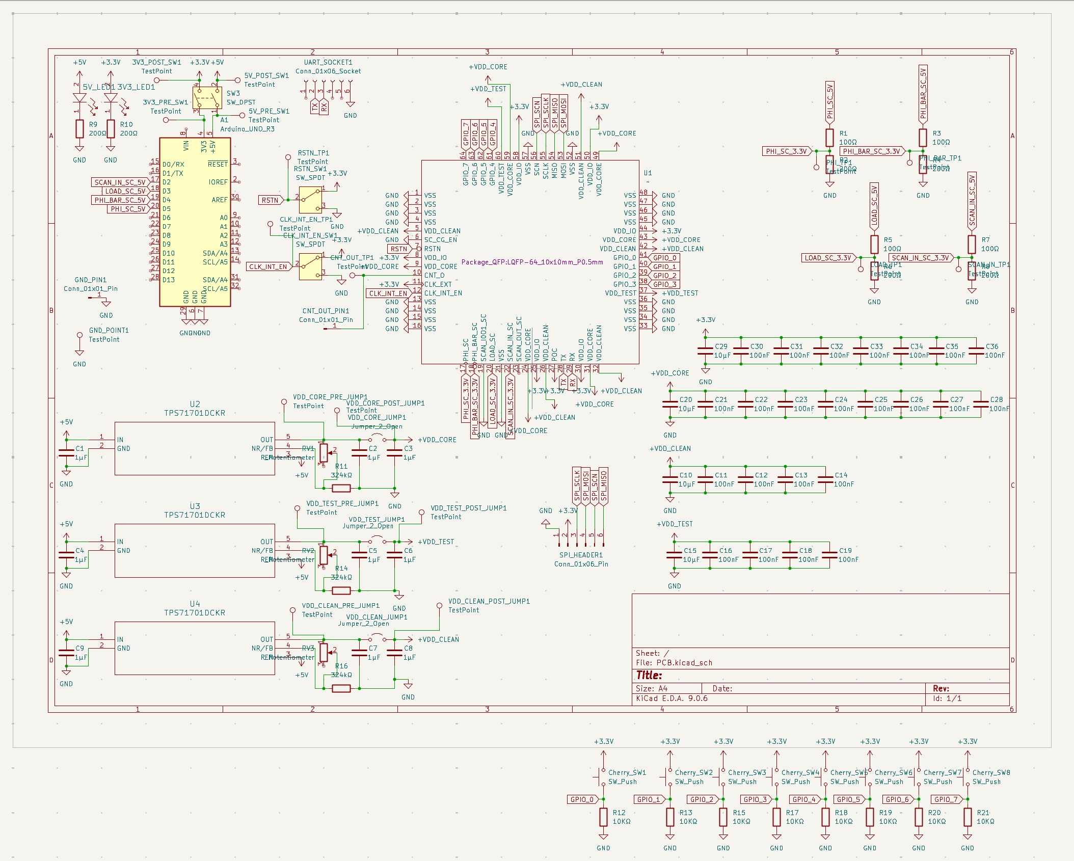
PCB Design
Before designing the PCB, we first validated the basic functionality of our system on a breadboard. This allowed us to quickly prototype the core components, verify signal correctness, and ensure that the chip interfaces behaved as expected. However, breadboard wiring is inherently limited in terms of signal integrity, power stability, reliability, and repeatability.
The purpose of creating a dedicated PCB is to provide a stable, well-structured, and electrically robust platform for testing our chip. The PCB ensures controlled routing, proper grounding, low-noise power distribution, and mechanically secure connections—all of which are essential for accurate measurement and characterization. It also integrates voltage regulators, test points, connectors, and peripheral interfaces in a clean and reproducible layout, enabling more complex experiments that would not be practical on a breadboard.
Overall, the PCB transforms the project from an early prototype into a reliable test and evaluation system, supporting systematic bring-up, debugging, and performance testing of the chip.
Assembled PCB Overview
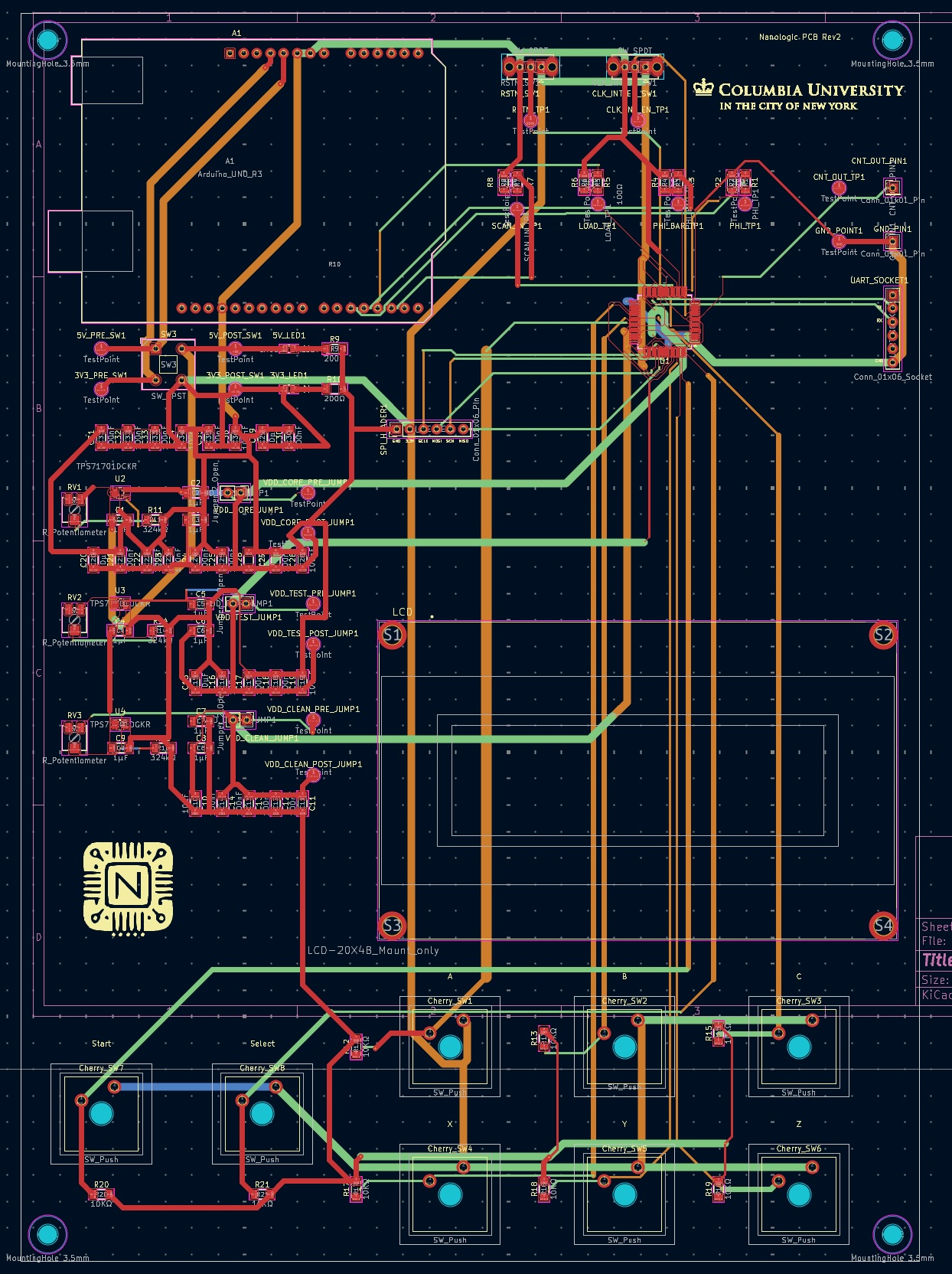
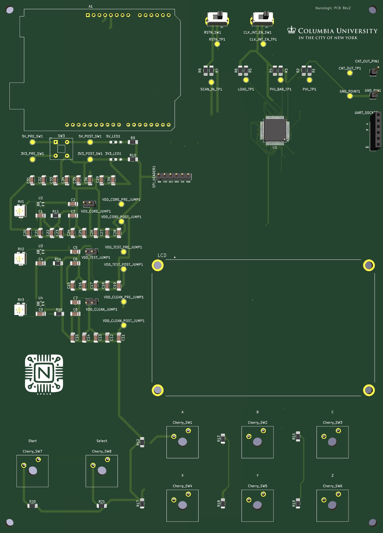
Board Architecture
The PCB is organized around the custom test chip placed at the center of the board, with all critical signals and supplies fanning out symmetrically. On the left side, an Arduino-UNO-compatible header provides a convenient digital interface for configuration, scan control, and simple firmware development. Around the chip, dedicated connectors expose scan, load, clock, and GPIO pins for lab instrumentation and external measurement.
The lower portion of the board is reserved for the power-management section, where the LDO regulators and associated jumpers, test points, and decoupling networks are grouped together. Along the bottom edge, an array of Cherry MX push buttons is connected to the chip GPIOs through pull-down resistors, forming a simple and robust user input interface. Mechanical features such as mounting holes and the reserved LCD area are aligned with the board outline so that the complete system can be mounted in a chassis or demo fixture. This layout keeps high-current power paths short, separates digital I/O from sensitive supply routing, and makes probing and debugging straightforward during bring-up.
PCB Top Layout
PCB Bottom Layout
Power Distribution
The board is powered from a 5 V input, which is locally regulated down to several on-board supply rails. Three TPS7A7100 LDO regulators generate the main voltages used by the chip: VDD_CORE, VDD_CLEAN, and VDD_TEST. Each regulator has its own input filter, adjustable feedback network, and output decoupling, allowing the core, clean, and test domains to be powered independently and tuned to the required voltage levels.
For measurement and bring-up, every rail is routed through “pre” and “post” jumpers and dedicated test points. This allows an ammeter or shunt resistor to be inserted in series with the supply to monitor per-domain current consumption without modifying the PCB. Banks of bulk (10 µF) and high-frequency (100 nF) capacitors are placed close to the test chip pins on each rail to reduce supply noise and stabilize the regulators. The 3.3 V logic domain used by the GPIO switches and external connectors is kept separate from the core supplies, ensuring that digital I/O activity does not disturb the more sensitive core and clean power domains. Together, this power-distribution scheme provides flexible, low-noise, and well-observable supplies for detailed silicon characterization.
PCB Rendering
Demonstration
We have three parts of our demo, all of which run on our custom SoC and share a common hardware and software backbone. At reset, the top-level program in demo.c initializes the UART, GPIO block, SPI controller, and the SPI-attached character LCD, then hands control over to a simple menu system. Every interaction with the board, from pressing buttons to reading status on the LCD or streaming numbers over UART, flows through this one main loop. The purpose of the design is to exercise distinct parts of the system in realistic ways: the UART and arithmetic datapath through the prime and π demos, and the GPIO, timers, and LCD through an interactive reaction game. Together they give a quick but thorough sanity check that the CPU, its peripherals, and the board integration are behaving correctly.
The code is organized into five source files. The entry point is demo.c, which pulls in the other four modules and contains the main polling loop and mode-selection logic. The menu and welcome-screen routines live in demo_menu.c, which is responsible for drawing the static text that introduces the board and lists the available demos. Numeric computation is split into two self-contained modules: demo_prime.c implements a prime-number generator and UART output routine, and demo_pi.c implements an integer-only spigot algorithm for π, again driving the UART. Finally, demo_game.c contains the reaction game, including its difficulty selection, scoring, timing, and game-over behavior. By compiling these together and letting demo.c call into each one, we keep each demo’s logic relatively self-contained while still sharing a common hardware abstraction layer.
User interaction starts with the menu code. demo_menu.c configures a short LCD delay and defines the strings used for the welcome message and menu lines. On boot, print_welcome_message() clears the display and prints “Hello Apple” on the first line and “This is NanoLogic!” on the second line, using two string fragments to fit the LCD’s width. After a brief pause, print_menu_options() redraws the screen to show the text “Choose from below:” at the top, followed by three labeled options on subsequent rows: “A:Print Prime (UART)”, “B:Play Game”, and “C:Print π (UART)”. The π symbol is rendered using a single custom character with value 0xF7. These routines don’t handle any input themselves; they simply establish the visual framing for the demos and then return to the main loop in demo.c.
The main program in demo.c wires this menu to the physical buttons. It defines small helper functions button_A(), button_B(), and button_C() that read GPIO pins 0–2 for the three primary options, and button_Select() on GPIO 7 for a “menu” or “select” action. The reaction game itself uses two additional GPIOs: GPIO 6 as a Start button and GPIO 7 as a Stop/Menu button, with corresponding helpers game_started() and game_stopped() in demo_game.c. After initialization and the welcome screen, main() prints the menu once and then enters an infinite polling loop. Within that loop, pressing the B button drops into the reaction-game mode; pressing A launches the prime-printing demo up to a fixed bound; pressing C launches the π demo; and pressing the Select/Menu button at any time just redraws the menu. Each demo runs to completion and then returns to main(), which clears or refreshes the LCD and continues waiting for the next button press.
The prime-number demonstration in demo_prime.c is a straightforward arithmetic stress test for the CPU and the UART. The core of the module is is_prime(unsigned int n), which checks primality using simple trial division: it rejects values below 2 and even numbers greater than 2, then tests odd divisors from 3 up to i * i <= n. The helper uart_print_number() converts an unsigned integer into ASCII without using any dynamic memory or library formatting routines. It repeatedly extracts base-10 digits into a small local buffer (in reverse order) and then emits them back out from most-significant to least-significant digit using uart_putc(), inserting a short delay between characters so the output is human-readable over a slow terminal. The top-level function print_primes_uart(unsigned int max_n) simply loops from 2 up to max_n, calls is_prime() on each candidate, and for every prime prints its decimal representation followed by a space and a longer delay to separate primes. From the user’s perspective, choosing the prime demo (button A) causes demo.c to clear the LCD, print “Printing” on the first line and “Primes…” on the second, and then call print_primes_uart(1000), which generates all primes up to 1000 on the UART. When that loop finishes, the code sends a newline, calls print_menu_options() again, and returns to the idle polling loop.
The π demo in demo_pi.c plays a similar role but exercises more complicated integer math. It is built around a spigot algorithm that generates digits of π without any floating-point operations. A global integer array pi_state[] of length PI_SPIGOT_LEN (computed as (PI_DIGITS_MAX * 10 / 3) + 1) holds the internal remainder state. The helper uart_emit_digit() takes a single digit, outputs its ASCII representation over UART with a small delay, and keeps track of how many digits have been written so far. After the very first digit it automatically inserts a decimal point, so the stream appears as “3.14159…”. The main routine print_pi_uart(int digits) initializes pi_state[] (each entry set to 2), then runs the standard spigot inner loop: for each output digit it walks the remainder array from the end toward the beginning, multiplies by 10, adds a carry term, divides by (2*i - 1), and stores the new remainder and carry. It keeps track of predigit and a run of trailing 9s so that when a carry turns the next digit into 10, it can increment the previous digit and flush the buffered 9s correctly, producing an accurate decimal expansion. Each finalized digit is passed through uart_emit_digit(), and after all requested digits it prints a newline and a long delay. When the user selects the π demo via button C, demo.c clears the LCD, prints “Calculating” followed by the π glyph and a few dots, calls print_pi_uart(PI_DIGITS_MAX) (up to 500 digits), and finally restores the menu once the UART output is complete. This mode is particularly useful for stressing repeated multiplication, division, and tight looping in the CPU’s datapath.
The reaction game in demo_game.c is the most interactive of the three and exists primarily to exercise GPIO input, timer peripherals, and SPI-driven LCD output under a more dynamic workload. The game assumes six “letter” buttons corresponding to GPIO bits 0–5, labeled on the screen using the single-character strings “A”, “B”, “C”, “X”, “Y”, and “Z”. Two additional GPIO lines serve as Start (bit 6) and Stop/Menu (bit 7). On the LCD, the game maintains two status lines: a score line initialized to “Score: 0000” and a lives line initialized to “Lives: 3”. Helper routines such as write_number_to_buffer(), update_score_line(), and update_lives_line() update these strings in place and reprint them at fixed rows on the LCD without any heap allocation. The difficulty display uses three static strings—“Mode: Easy”, “Mode: Normal”, and “Mode: Hard”—and show_mode_line() draws the currently selected difficulty on the LCD’s second row.
When the user presses the B button from the main menu, demo.c enters a difficulty-selection screen. It clears the LCD, writes “React!” on the top line, shows the current mode (“Mode: Easy” by default), and prints a prompt line: “A=Easy B=Norm C=Hard” followed by “Press Game Start” on the last row. While the Start button is not yet pressed, the program polls the A, B, and C buttons: pressing A switches to Easy, B to Normal, and C to Hard. Each time the difficulty changes, show_mode_line() redraws only the mode line so the rest of the screen remains stable. Once the user presses Start (GPIO 6), the code briefly displays “Game Starting!”, calls reaction_game(hard_mode), and hands control over to the game loop.
Inside reaction_game(), both hardware timers are reset and started, the score is set to zero, and the lives counter is set to three. The game then enters an infinite series of rounds until the player either runs out of lives or explicitly exits to the menu. At the start of each round it reads the current values of the two timers, using them as simple entropy sources. For Easy mode, it chooses a single target letter by taking timer_read(0) % num_letters. For Normal mode, it chooses a first letter in the same way and a second, distinct letter using pick_second_letter(), which offsets the first index by a non-zero amount derived from the second timer and wraps around the six letters. For Hard mode, it calls build_hard_mask(), which mixes the two timer values into a bitmask representing a random subset of the six buttons (between one and six distinct letters). It then reconstructs an ordered list of those letters from the mask. In all cases, the chosen letters are displayed on the top row by show_round_header(), which uses build_display_string() to render them as a compact expression like “A+B+C” while simultaneously updating the score and lives lines below.
The input phase of each round is driven by polling and precise timing. A helper read_letter_mask() snapshots the low bits of the GPIO input register into a bitmask of currently pressed letter buttons. The round logic maintains a “wait budget” counter (ROUND_TIMEOUT_STEPS) and a reaction window (SIMUL_WINDOW_TICKS) measured by timer 0. Initially, the game waits for the player to press something: if no buttons are pressed, it decrements the wait budget, sleeps briefly, and repeats; if the budget reaches zero before any press is observed, the round is marked as “timed out.” Once at least one expected button is pressed, the game records the current timer value as the start of the reaction window and enters a second phase where it continuously checks that (1) no extra buttons outside the expected mask are pressed, and (2) the player eventually holds exactly the full expected combination within the allowed time. If the elapsed time exceeds SIMUL_WINDOW_TICKS or an extra button is detected at any point, the round is treated as a miss. At any time, pressing the Stop/Menu button (GPIO 7) invokes show_game_over_screen(), which displays “Game Over :(” together with the final score and a prompt “Start=Retry Sel=Menu”; the subsequent button press determines whether the game restarts from scratch or returns to the main menu.
At the end of the polling loop for a round, the game decides whether the input was correct. If the pressed mask matches the expected mask within the reaction window, it increments the score by one, updates the score line on the LCD, clears the top row, prints “Correct!”, and waits briefly so the player can see the feedback. If the player timed out or pressed the wrong combination, the code decrements the lives counter (down to a minimum of zero), updates the lives line, and prints either “Too Slow” or “Wrong:(” on the top row depending on the cause. After another short pause, if lives have dropped to zero, the game shows the game-over screen and either restarts or exits based on the user’s choice; otherwise it simply moves on to the next round with a new random letter pattern. When reaction_game() finally returns, demo.c prints “Returning to Menu” on the LCD, waits briefly, and then calls print_menu_options() to put the system back into its initial menu state.
Taken together, these modules form a small but complete demonstration suite for the SoC. The menu and main loop in demo.c coordinate the other four components, the prime and π demos in demo_prime.c and demo_pi.c stress computation and UART output with purely integer algorithms, and the reaction game in demo_game.c keeps the GPIO, timers, and LCD busy with fast user interaction. Because each demo uses different combinations of peripherals and arithmetic primitives, having all three available behind the same simple front panel makes it easy to validate the hardware and to showcase the capabilities of the system to anyone sitting down in front of the board.
Demo Program Code
Demo Program:
demo.c (menu and mode control)
#include <stdint.h>
#include <stdbool.h>
#include "spi_lcd_driver.h"
#include "demo_game.c"
#include "demo_menu.c"
#include "demo_prime.c"
#include "demo_pi.c"

volatile uint8_t lcd_delay = 3;
volatile char str0[10] = "          ";
volatile char strnew1[6] = "React!";
volatile char strnew2[8] = "Printing";
volatile char strnew3[9] = "Primes...";
volatile char strnew4[16]  = "Press Game Start";
volatile char strnew5[14]  = "Game Starting!";
volatile char strnew6[17]  = "Returning to Menu";
volatile char strnew7[11] = "Calculating";
volatile char strnew8[1] = {0xF7};
volatile char strnew9[3] = "...";
volatile char str_mode_select[21] = "A=Easy B=Norm C=Hard";
int button_A() { return (gpio_pin_read() & (1 << 0)); }   // GPIO0 → A
int button_B() { return (gpio_pin_read() & (1 << 1)); }   // GPIO1 → B
int button_C() { return (gpio_pin_read() & (1 << 2)); }   // GPIO2 → C
int button_Select() { return (gpio_pin_read() & (1 << 7)); }   // GPIO7 → MENU

int main(void) {
    uart_init();
    gpio_init();
    spi_init();
    lcd_init(lcd_delay);

    setCursor(0, 0, lcd_delay);
    lcd_print(str0, 10, lcd_delay);

    print_welcome_message();
    delay(50000);
    print_menu_options();

     while (1)
    {
        // ------------------ OPTION 1: Play Game ------------------
        if (button_B()) {
            uint8_t hard_mode = DIFF_EASY;
            uint8_t drawn_mode = 2; // invalid sentinel to force initial draw

            clear();
            setCursor(0, 0, lcd_delay);
            lcd_print(strnew1, 6, lcd_delay);
            if (drawn_mode != hard_mode) {
                show_mode_line(hard_mode);
                drawn_mode = hard_mode;
            }
            setCursor(0, 2, lcd_delay);
            lcd_print(str_mode_select, 20, lcd_delay);
            setCursor(0, 3, lcd_delay);
            lcd_print(strnew4, 16, lcd_delay);
            while (!game_started()) {
                if (button_A() && hard_mode != DIFF_EASY) {
                    hard_mode = DIFF_EASY;
                    if (drawn_mode != hard_mode) {
                        show_mode_line(hard_mode);
                        drawn_mode = hard_mode;
                    }
                }
                if (button_B() && hard_mode != DIFF_NORMAL) {
                    hard_mode = DIFF_NORMAL;
                    if (drawn_mode != hard_mode) {
                        show_mode_line(hard_mode);
                        drawn_mode = hard_mode;
                    }
                }
                if (button_C() && hard_mode != DIFF_HARD) {
                    hard_mode = DIFF_HARD;
                    if (drawn_mode != hard_mode) {
                        show_mode_line(hard_mode);
                        drawn_mode = hard_mode;
                    }
                }
                delay(1000);
            }

            clear();
            setCursor(0,0,lcd_delay);
            lcd_print(strnew5, 14, lcd_delay);
            long_delay(1000);


            reaction_game(hard_mode);        // your full game logic

            clear();
            setCursor(0,0,lcd_delay);
            lcd_print(strnew6, 17, lcd_delay);
            long_delay(1000);

            clear();
            print_menu_options();   // return to menu
        }

        // ------------------ OPTION 2: Print Primes UART ------------------
        if (button_A()) {

            clear();
            setCursor(0, 0, lcd_delay);
            lcd_print(strnew2, 8, lcd_delay);
            setCursor(0, 1, lcd_delay);
            lcd_print(strnew3, 9, lcd_delay);

            print_primes_uart(1000);
            uart_putc('\n');


            print_menu_options();
        }
        if (button_C()) {
            clear();
            setCursor(0, 0, lcd_delay);
            lcd_print(strnew7, 11, lcd_delay);
            setCursor(0, 1, lcd_delay);
            lcd_print(strnew8, 1, lcd_delay);
            lcd_print(strnew9, 3, lcd_delay);
            print_pi_uart(PI_DIGITS_MAX);
            print_menu_options();
        }

        // ------------------ OPTION 3: Reprint menu ------------------
        if (button_Select()) {
            print_menu_options();
        }
    }

    return 0;
}
demo_game.c (reaction game)
volatile uint8_t lcd_delay_game = 3;
volatile char str1[1] = "A";
volatile char str2[1] = "B";
volatile char str3[1] = "C";
volatile char str4[1] = "X";
volatile char str5[1] = "Y";
volatile char str6[1] = "Z";
volatile char str7[8]  = "Correct!";
volatile char str8[7]  = "Wrong:(" ;
volatile char str9[16]  = "    Game Over :(";
volatile char str10[16]  = "Press Game Start";
volatile char str11[13]  = "Game Started!";
volatile char str_score_line[12] = "Score: 0000";
volatile char str_lives_line[9] = "Lives: 3";
volatile char str_timeout[9] = "Too Slow";
volatile char str_mode_easy[11] = "Mode: Easy";
volatile char str_mode_normal[13] = "Mode: Normal";
volatile char str_mode_hard[11] = "Mode: Hard";
volatile char str_gameover_prompt[21] = "Start=Retry Sel=Menu";
volatile char blank_line[21] = "                    ";
volatile char* letters[6] = {str1, str2, str3, str4, str5, str6};
uint8_t num_letters = 6;
#define DIFF_EASY   0
#define DIFF_NORMAL 1
#define DIFF_HARD   2
#define SIMUL_WINDOW_TICKS 6000000U
#define ROUND_TIMEOUT_STEPS 125
int game_started() {
    uint32_t val = gpio_pin_read() & 0xFF;
    return (val & (1 << 6)) != 0; // GPIO 6 = START
}

int game_stopped() {
    uint32_t val = gpio_pin_read() & 0xFF;
    return (val & (1 << 7)) != 0; // GPIO 7 = STOP
}

int get_pressed_button() {
    uint32_t val = gpio_pin_read() & 0xFF; // Read 8-bit GPIO PADIN
    for (int i = 0; i < num_letters; i++) {
        if (val & (1 << i)) {       // Active HIGH buttons
            return i;
        }
    }
    return -1;
}

// Write an integer into a pre-sized buffer without heap/float usage.
static void write_number_to_buffer(uint32_t value, volatile char *buffer, uint8_t offset, uint8_t digits) {
    for (uint8_t i = 0; i < digits; i++) {
        buffer[offset + digits - 1 - i] = (char)('0' + (value % 10));
        value /= 10;
    }
}

static uint8_t read_letter_mask() {
    return (uint8_t)(gpio_pin_read() & ((1U << num_letters) - 1U));
}

static void clear_row(uint8_t row) {
    setCursor(0, row, lcd_delay_game);
    lcd_print(blank_line, 20, lcd_delay_game);
    setCursor(0, row, lcd_delay_game);
}

static void update_score_line(uint32_t score) {
    if (score > 9999U) {
        score = 9999U; // clamp to displayed width
    }
    write_number_to_buffer(score, str_score_line, 7, 4);
    setCursor(0, 2, lcd_delay_game);
    lcd_print(str_score_line, 11, lcd_delay_game);
}

static void update_lives_line(uint32_t lives) {
    if (lives > 9U) {
        lives = 9U;
    }
    str_lives_line[7] = (char)('0' + lives);
    setCursor(0, 3, lcd_delay_game);
    lcd_print(str_lives_line, 8, lcd_delay_game);
}

static void show_mode_line(uint8_t hard_mode) {
    clear_row(1);
    setCursor(0, 1, lcd_delay_game);
    if (hard_mode == DIFF_EASY) lcd_print(str_mode_easy, 10, lcd_delay_game);
    else if (hard_mode == DIFF_NORMAL) lcd_print(str_mode_normal, 12, lcd_delay_game);
    else lcd_print(str_mode_hard, 10, lcd_delay_game);
}

static int pick_second_letter(int first_letter, uint32_t random_val) {
    int offset = (int)(random_val % (num_letters - 1)) + 1; // 1..num_letters-1
    return (first_letter + offset) % num_letters;
}

static uint8_t build_hard_mask(uint32_t seed0, uint32_t seed1, int *letters_out) {
    uint8_t count = (uint8_t)((seed1 % num_letters) + 1); // 1..6
    uint32_t mix = seed0 ^ (seed1 << 1);
    uint8_t mask = 0;
    for (uint8_t i = 0; i < count; i++) {
        int candidate = (int)((mix >> (i * 3)) % num_letters);
        uint8_t tries = 0;
        while ((mask & (1U << candidate)) && tries < num_letters) {
            candidate = (candidate + 1) % num_letters;
            tries++;
        }
        letters_out[i] = candidate;
        mask |= (uint8_t)(1U << candidate);
    }
    return mask;
}

static void build_display_string(const int *letters_list, uint8_t count, char *buf, uint8_t *out_len) {
    uint8_t idx = 0;
    for (uint8_t i = 0; i < count; i++) {
        buf[idx++] = letters[letters_list[i]][0];
        if (i + 1 < count) {
            buf[idx++] = '+';
        }
    }
    *out_len = idx;
}

static void show_round_header(const int *letters_list, uint8_t count, uint32_t score, uint32_t lives) {
    clear_row(0);
    setCursor(0, 0, lcd_delay_game);
    char display_buf[12];
    uint8_t disp_len = 0;
    build_display_string(letters_list, count, display_buf, &disp_len);
    lcd_print(display_buf, disp_len, lcd_delay_game);
    update_score_line(score);
    update_lives_line(lives);
}

static uint8_t wait_for_retry_or_menu() {
    while (game_started() || game_stopped()) {
        delay(500);
    }
    while (1) {
        if (game_started()) return 1;
        if (game_stopped()) return 0;
        delay(500);
    }
}

static uint8_t show_game_over_screen(uint32_t final_score) {
    if (final_score > 9999U) {
        final_score = 9999U;
    }
    write_number_to_buffer(final_score, str_score_line, 7, 4);
    clear();
    setCursor(0, 0, lcd_delay_game);
    lcd_print(str9, 16, lcd_delay_game);
    lcd_print(str9, 4, lcd_delay_game);
    setCursor(0, 2, lcd_delay_game);
    lcd_print(str_score_line, 11, lcd_delay_game);
    setCursor(0, 3, lcd_delay_game);
    lcd_print(str_gameover_prompt, 20, lcd_delay_game);
    return wait_for_retry_or_menu();
}

void reaction_game(uint8_t difficulty) {
restart_game:
    timer_reset_and_start(0);
    timer_reset_and_start(1);
    uint32_t score = 0;
    uint32_t lives = 3;
    clear();
    show_mode_line(difficulty);
    update_score_line(score);
    update_lives_line(lives);
    int target_letters[6];
    while (1) {
        uint32_t t = timer_read(0);
        uint32_t t_alt = timer_read(1);

        uint8_t expected_mask = 0;
        uint8_t target_count = 1;
        target_letters[0] = (int)(t % num_letters);
        if (difficulty == DIFF_NORMAL) {
            target_count = 2;
            target_letters[1] = pick_second_letter(target_letters[0], t_alt);
            expected_mask = (uint8_t)((1U << target_letters[0]) | (1U << target_letters[1]));
        } else if (difficulty == DIFF_HARD) {
            expected_mask = build_hard_mask(t, t_alt, target_letters);
            target_count = 0;
            for (uint8_t i = 0; i < num_letters; i++) {
                if (expected_mask & (1U << i)) {
                    target_letters[target_count++] = i;
                }
            }
        } else {
            expected_mask = (uint8_t)(1U << target_letters[0]);
            target_count = 1;
        }

        show_round_header(target_letters, target_count, score, lives);
        uint8_t pressed_mask = 0;
        uint8_t input_correct = 0;
        uint8_t saw_press = 0;
        uint32_t window_start = 0;
        uint32_t wait_budget = ROUND_TIMEOUT_STEPS;
        uint8_t timed_out = 0;
        while (1) {
            if (game_stopped()) {
                if (show_game_over_screen(score)) {
                    goto restart_game;
                }
                return;    // Exit to menu
            }

            pressed_mask = read_letter_mask();
            if (!saw_press) {
                if (pressed_mask == 0) {
                    if (wait_budget == 0) {
                        timed_out = 1;
                        break;
                    }
                    wait_budget--;
                    delay(500);
                    continue;
                }
                if ((pressed_mask & ~expected_mask) != 0) {
                    break; // Extra buttons pressed (cheating)
                }
                saw_press = 1;
                window_start = timer_read(0);
            } else {
                if ((uint32_t)(timer_read(0) - window_start) > SIMUL_WINDOW_TICKS) {
                    break; // took too long to complete combo
                }
                if ((pressed_mask & ~expected_mask) != 0) {
                    break; // Extra buttons pressed (cheating)
                }
            }
            if (pressed_mask == expected_mask) {
                input_correct = 1;
                break;
            }
        }

        if (input_correct) {
            score++;
            update_score_line(score);
            clear_row(0);
            setCursor(0, 0, lcd_delay_game);
            lcd_print(str7, 8, lcd_delay_game);
            long_delay(1000);
        }
        else {
            if (lives > 0) {
                lives--;
            }
            update_lives_line(lives);
            clear_row(0);
            setCursor(0, 0, lcd_delay_game);
            if (timed_out) {
                lcd_print(str_timeout, 8, lcd_delay_game);
            } else {
                lcd_print(str8, 7, lcd_delay_game);
            }
            long_delay(1000);
        }

        long_delay(1000); // Adjust delay as needed
        if (lives == 0) {
            if (show_game_over_screen(score)) {
                goto restart_game;
            }
            return;
        }
    }
}
demo_menu.c (LCD menu)
volatile uint8_t lcd_delay_menu = 3;
volatile char str1a[9] = "Hello App";
volatile char str1b[3] = "le!";
volatile char str2a[12] = "This is Nano";
volatile char str2b[6] = "Logic!";
volatile char str3a[6] = "Choose";
volatile char str3b[5] = " from";
volatile char str3c[7] = " below:";

volatile char str4a[7] = "A:Print";
volatile char str4b[6] = " Prime";
volatile char str4c[7] = " (UART)";

volatile char str5a[6] = "B:Play";
volatile char str5b[5] = " Game";

volatile char str6a[8] = "C:Print ";
volatile char str6b[1] = {0xF7};
volatile char str6c[7] = " (UART)";
void print_welcome_message() {

  clear();
  setCursor(0, 0, lcd_delay_menu);
  lcd_print(str1a, 9, lcd_delay_menu);
  lcd_print(str1b, 3, lcd_delay_menu);

  setCursor(0, 1, lcd_delay_menu);
  lcd_print(str2a, 12, lcd_delay_menu);
  lcd_print(str2b, 6, lcd_delay_menu);
  long_delay(1000);

}

void print_menu_options () {

  clear();

  lcd_print(str3a, 6, lcd_delay_menu);
  lcd_print(str3b, 5, lcd_delay_menu);
  lcd_print(str3c, 7, lcd_delay_menu);


  setCursor(0, 1, lcd_delay_menu);
  lcd_print(str4a, 7, lcd_delay_menu);
  lcd_print(str4b, 6, lcd_delay_menu);
  lcd_print(str4c, 7, lcd_delay_menu);

  setCursor(0, 2, lcd_delay_menu);
  lcd_print(str5a, 6, lcd_delay_menu);
  lcd_print(str5b, 5, lcd_delay_menu);

  setCursor(0, 3, lcd_delay_menu);
  lcd_print(str6a, 8, lcd_delay_menu);
  lcd_print(str6b, 1, lcd_delay_menu);
  lcd_print(str6c, 7, lcd_delay_menu);
  long_delay(1000);
}
demo_prime.c (UART prime generator)
// -------------------------------------------------
// Prime check
// -------------------------------------------------
int is_prime(unsigned int n) {
    if (n < 2) return 0;
    if (n == 2) return 1;
    if (n % 2 == 0) return 0;

    for (unsigned int i = 3; i * i <= n; i += 2) {
        if (n % i == 0) return 0;
    }
    return 1;
}

// -------------------------------------------------
// Print integer as characters over UART using uart_putc()
// -------------------------------------------------
void uart_print_number(unsigned int n) {
    char digits[10];
    int i = 0;

    // Extract digits (reverse)
    while (n > 0) {
        digits[i++] = (n % 10) + '0';
        n /= 10;
    }

    // Print in correct order
    while (--i >= 0) {
        uart_putc(digits[i]);
        delay(30);
    }
}

// -------------------------------------------------
// Print all primes ≤ max_n using UART
// -------------------------------------------------
void print_primes_uart(unsigned int max_n) {
    for (unsigned int n = 2; n <= max_n; n++) {
        if (is_prime(n)) {

            uart_print_number(n);    // Send digits
            uart_putc(' ');          // Space after each prime
            delay(300);
        }
    }
}
demo_pi.c (UART pi digits)
// Spigot-based digit generator for pi (integer-only, no FP needed).
// The CPU is 32-bit, so keep buffers small; this prints up to PI_DIGITS_MAX digits.

#define PI_DIGITS_MAX 500
#define PI_SPIGOT_LEN ((PI_DIGITS_MAX * 10 / 3) + 1)

static int pi_state[PI_SPIGOT_LEN];

// Emit a single digit over UART and drop a decimal point after the first digit.
static void uart_emit_digit(int digit, int *digits_written) {
    uart_putc((char)('0' + digit));
    delay(10);

    (*digits_written)++;
    if (*digits_written == 1) {     // after leading '3'
        uart_putc('.');
        delay(50);
    }
}

// Generate and print `digits` digits of pi (including the leading '3').
static void print_pi_uart(int digits) {
    if (digits < 1) return;

    // Initialize spigot state
    for (int i = 0; i < PI_SPIGOT_LEN; i++) {
        pi_state[i] = 2;
    }

    int nines = 0;
    int predigit = 0;
    int digits_written = 0;

    for (int j = 0; j < digits; j++) {
        int carry = 0;

        // Core spigot step: update the remainder array.
        for (int i = PI_SPIGOT_LEN; i > 0; i--) {
            int idx = i - 1;
            int x = pi_state[idx] * 10 + carry * i;
            pi_state[idx] = x % (2 * i - 1);
            carry = x / (2 * i - 1);
        }

        int current_digit = carry / 10;
        pi_state[0] = carry % 10;

        // The first digit is just staged; others are emitted with carry handling.
        if (j == 0) {
            predigit = current_digit;
            continue;
        }

        if (current_digit == 9) {
            nines++;
        } else if (current_digit == 10) {
            uart_emit_digit(predigit + 1, &digits_written);
            for (int k = 0; k < nines; k++) {
                uart_emit_digit(0, &digits_written);
            }
            predigit = 0;
            nines = 0;
        } else {
            uart_emit_digit(predigit, &digits_written);
            for (int k = 0; k < nines; k++) {
                uart_emit_digit(9, &digits_written);
            }
            predigit = current_digit;
            nines = 0;
        }
    }

    uart_emit_digit(predigit, &digits_written);
    for (int k = 0; k < nines; k++) {
        uart_emit_digit(9, &digits_written);
    }

    uart_putc('\n');
    delay(10000);
}
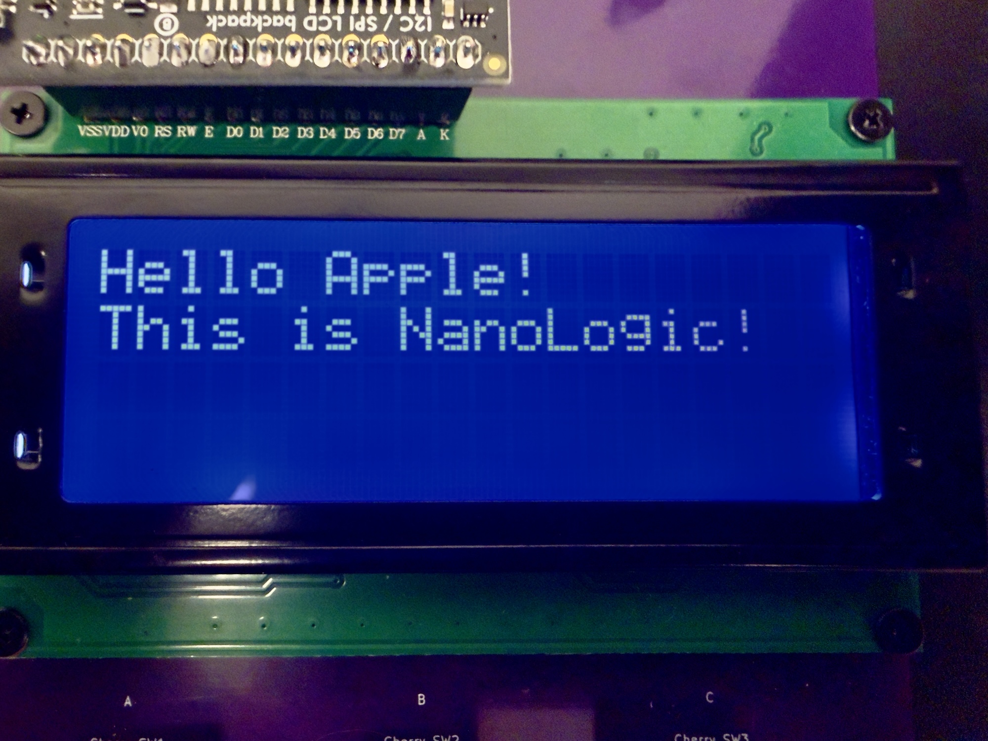
Demo Menu on LCD
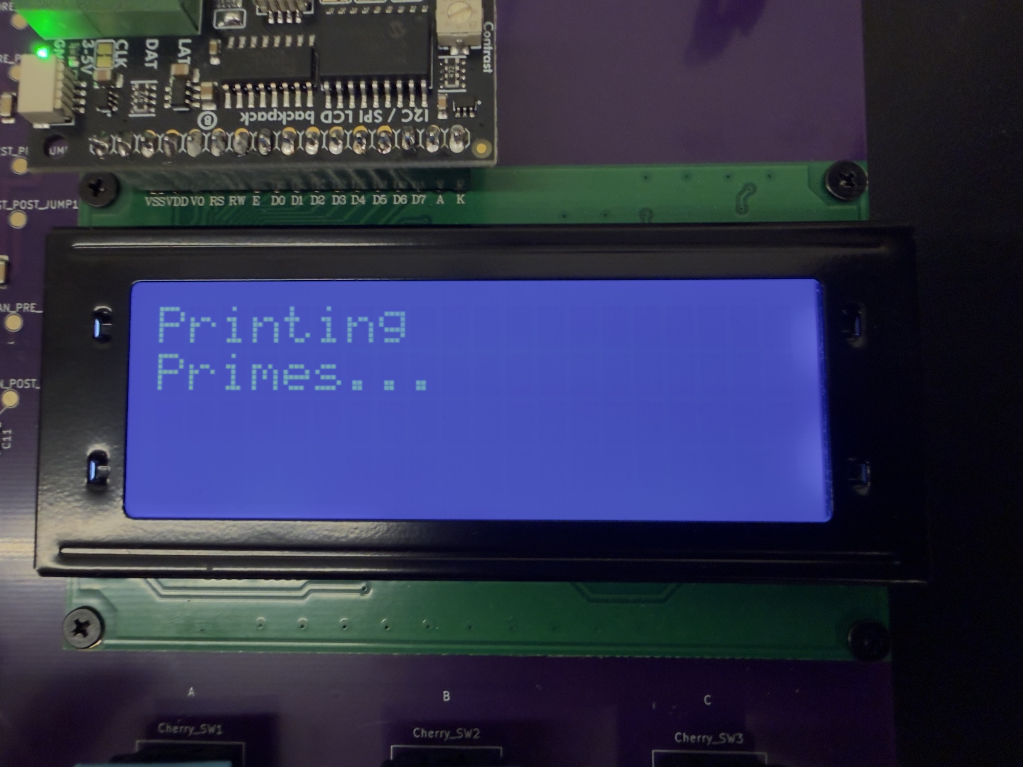
Prime Demo on LCD
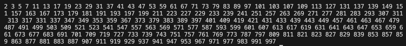
Prime Demo Output over UART
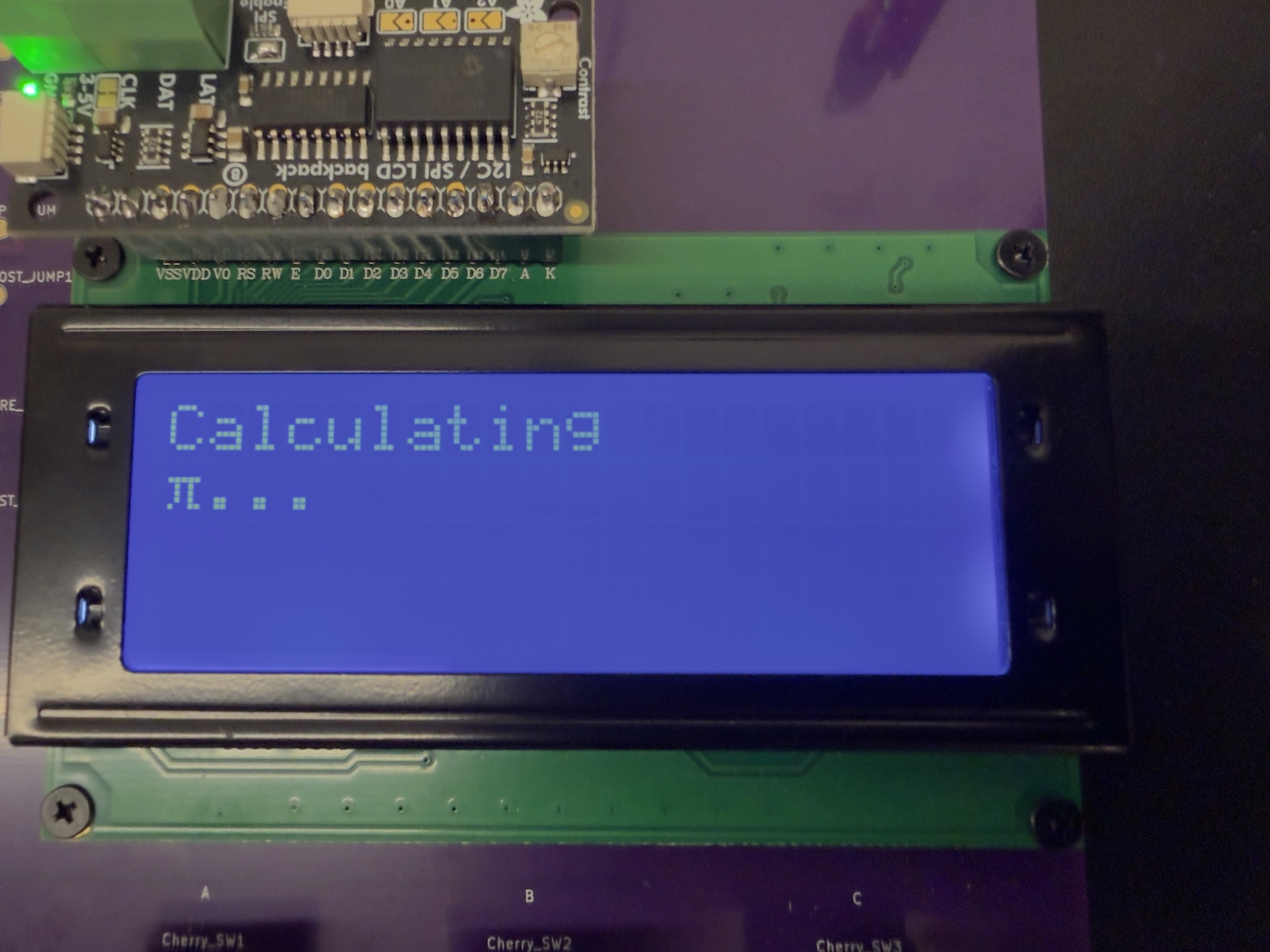
Pi Demo on LCD

Pi Demo Output over UART
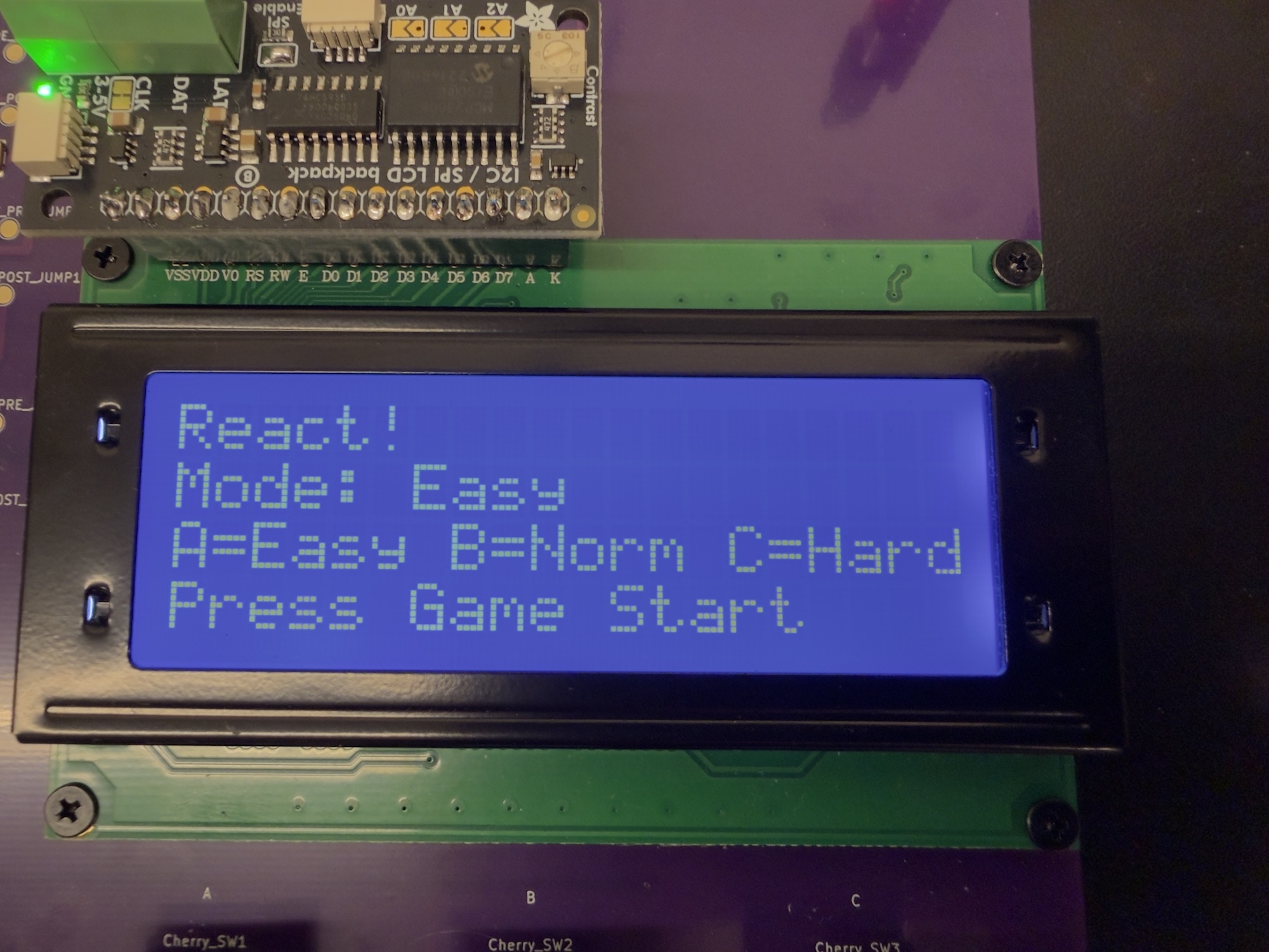
Game Mode Selection
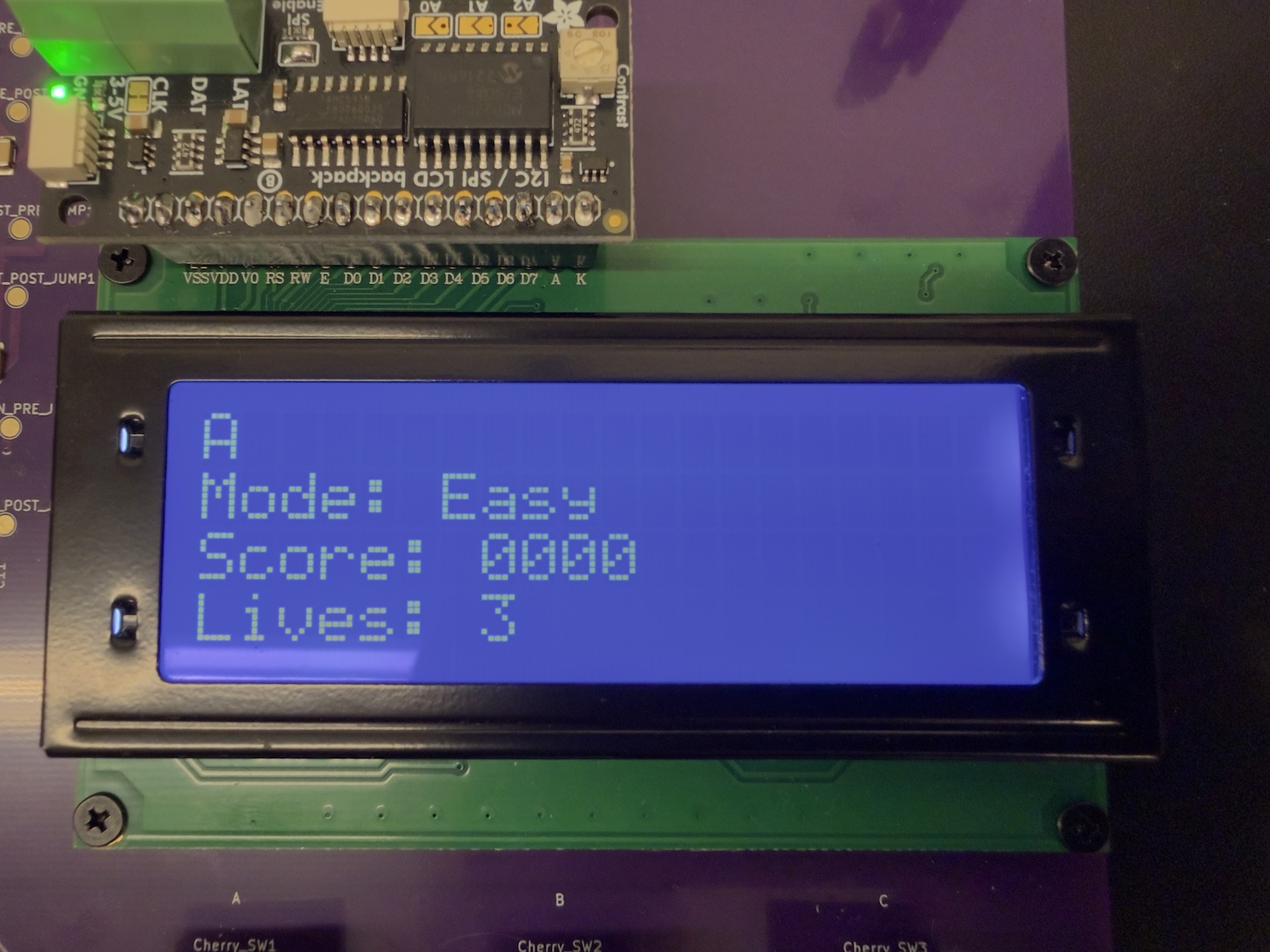
Game Easy Mode
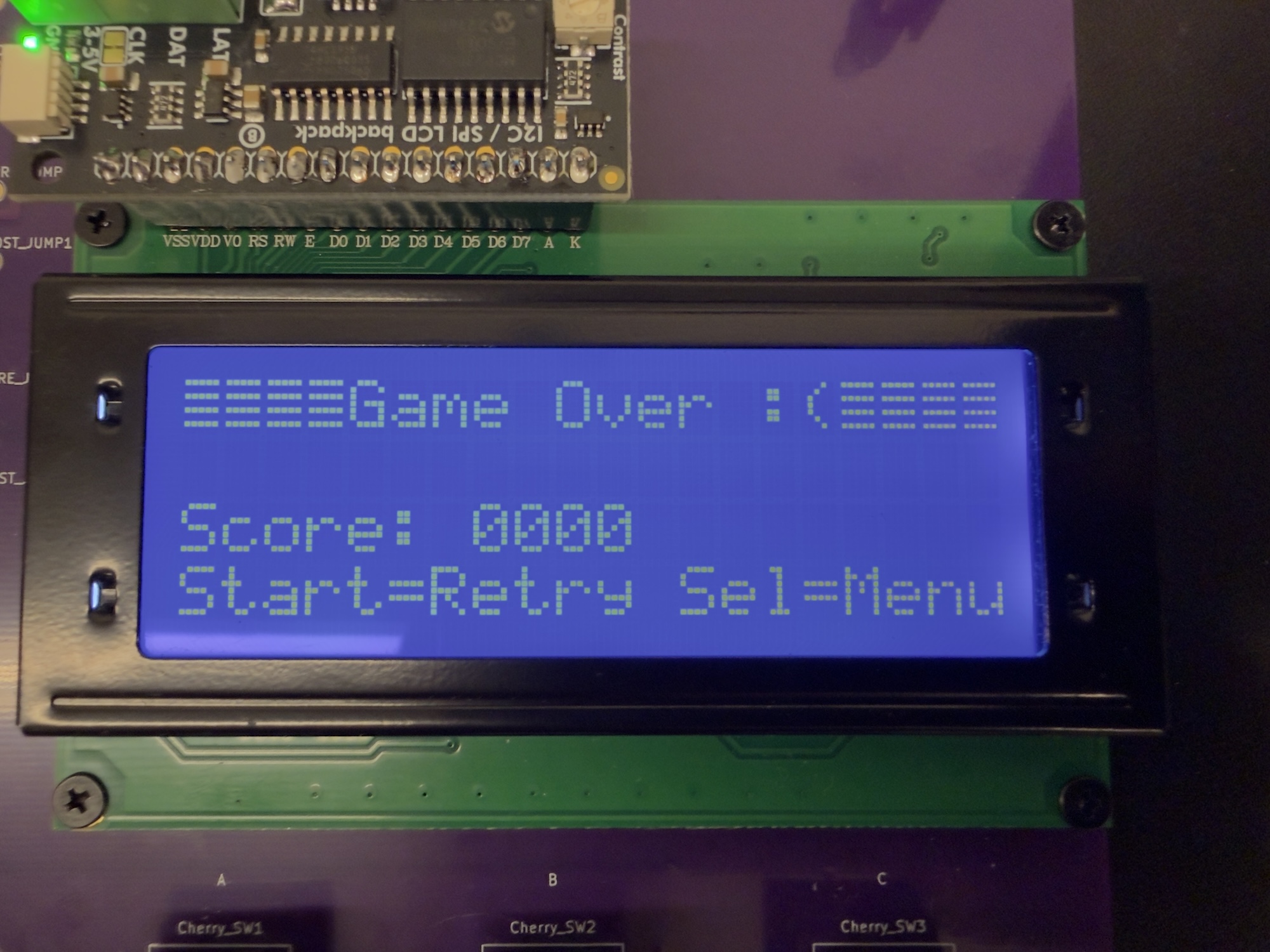
Game Over Screen
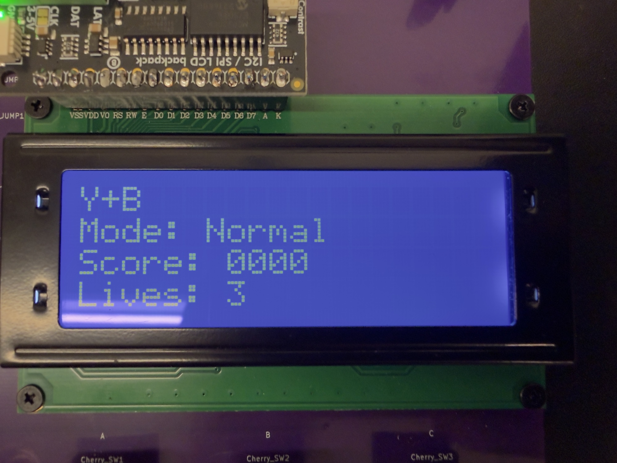
Game Normal Mode
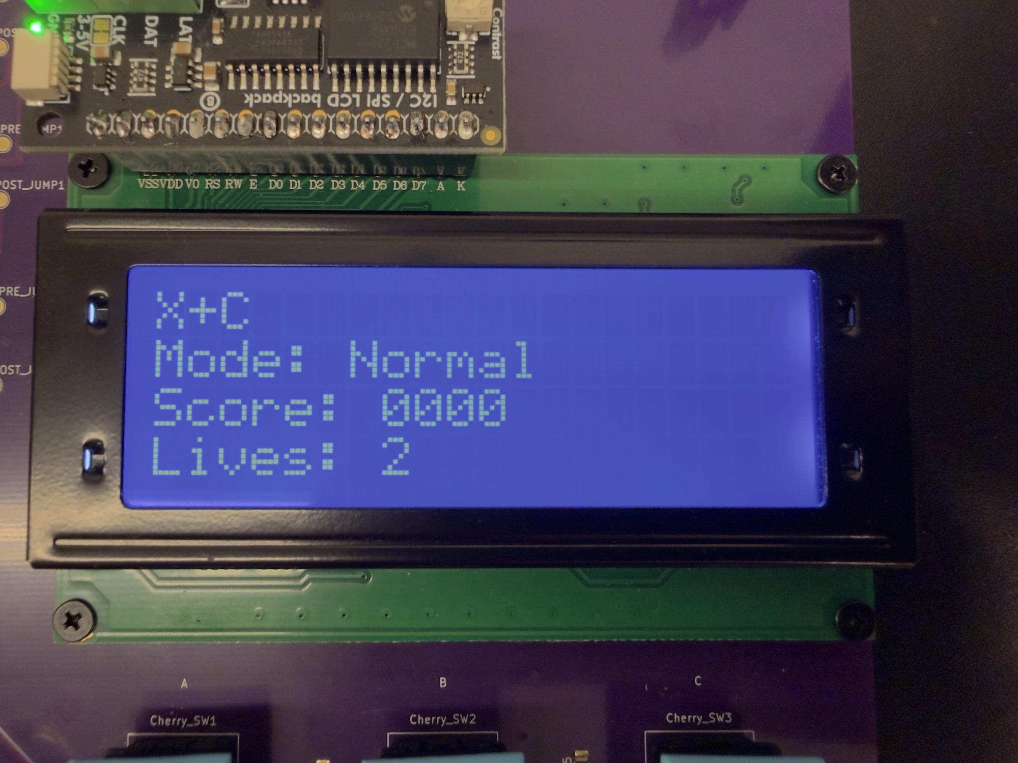
Game Normal Mode In Progress
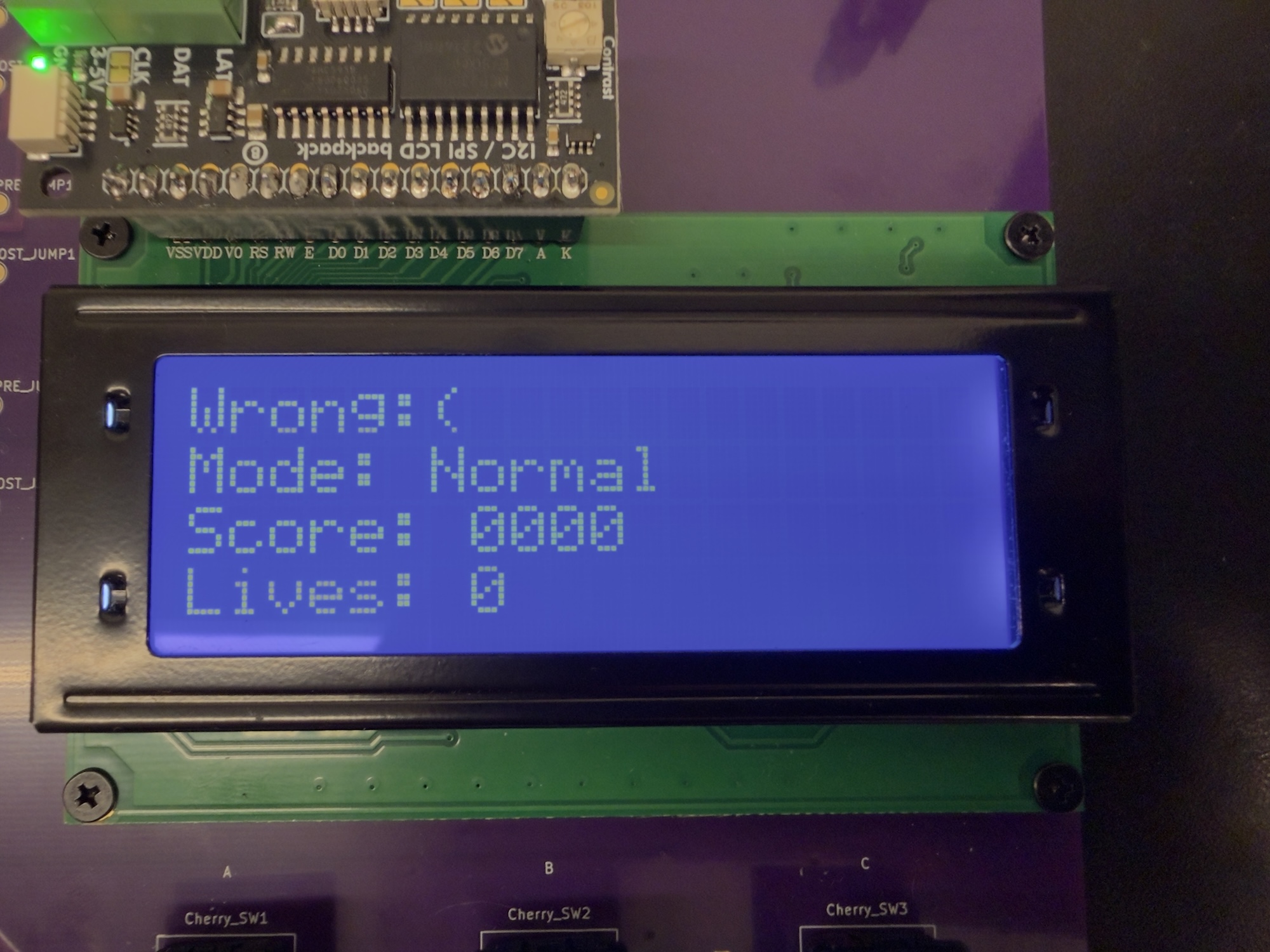
Game Normal Mode Incorrect Input
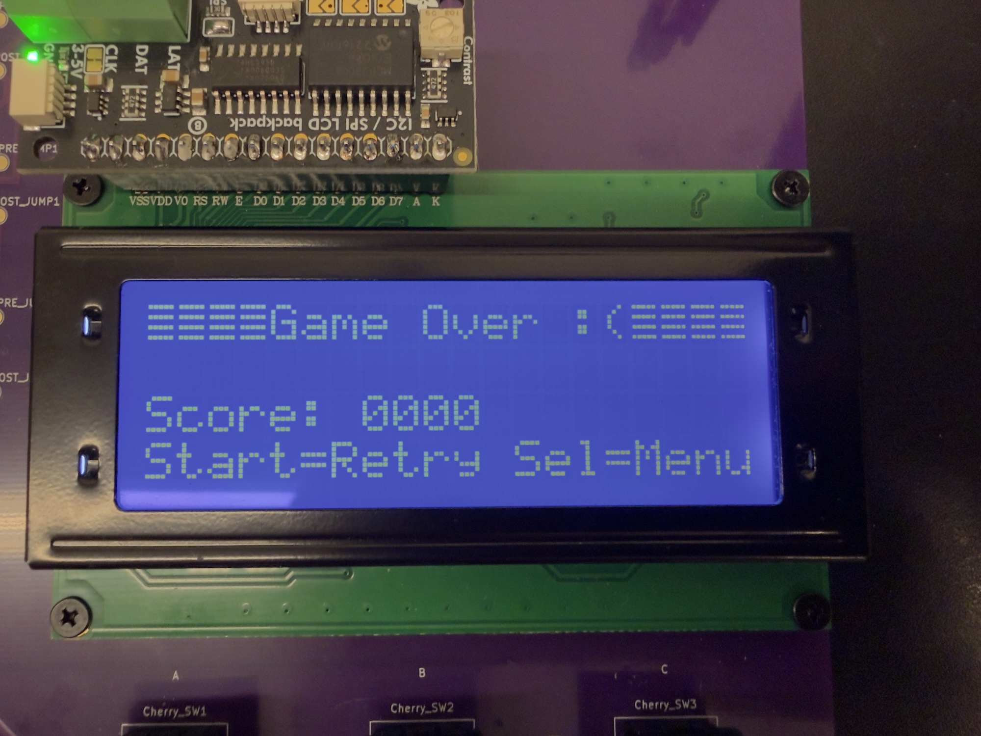
Game Normal Mode Over
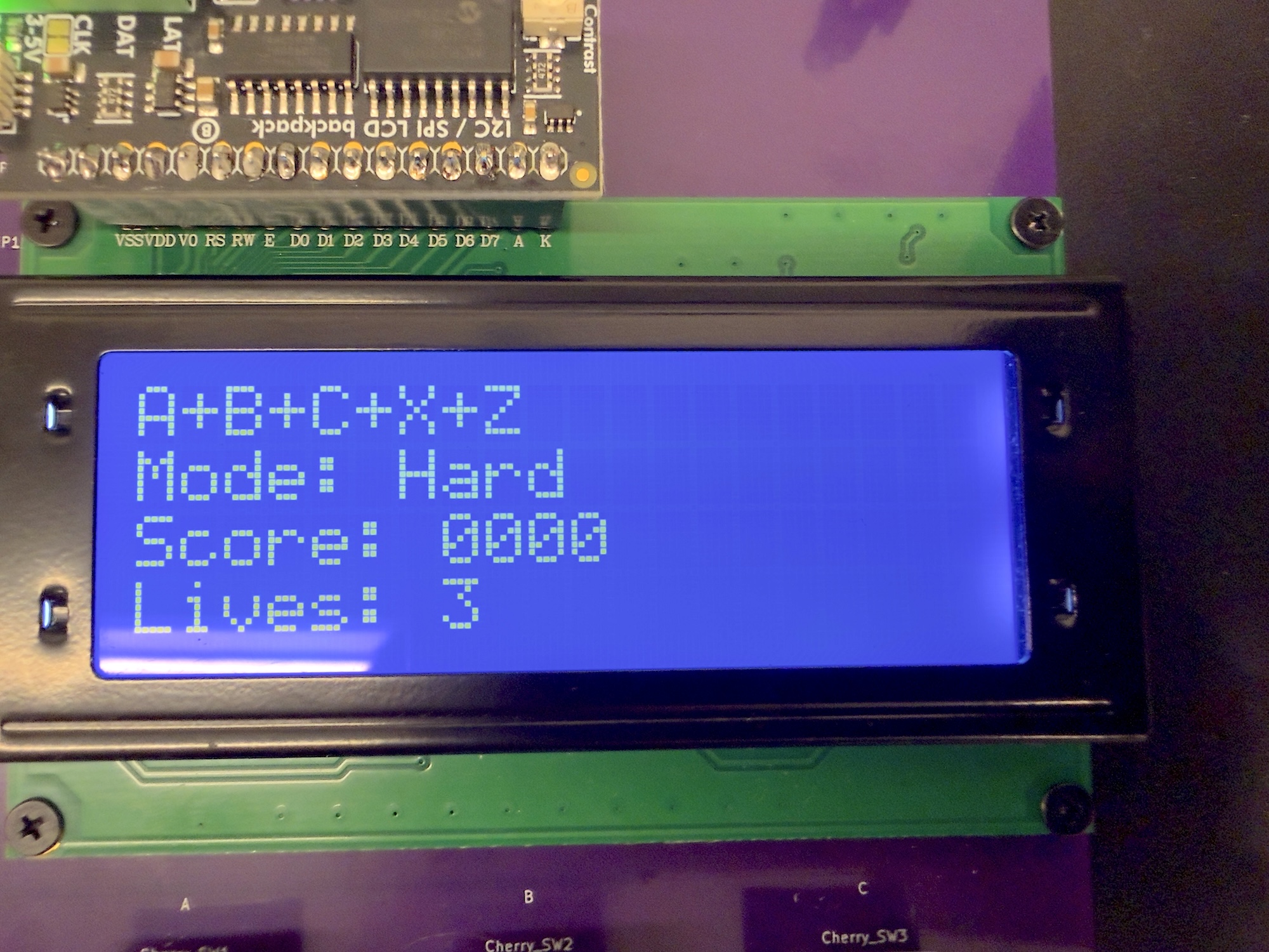
Game Hard Mode
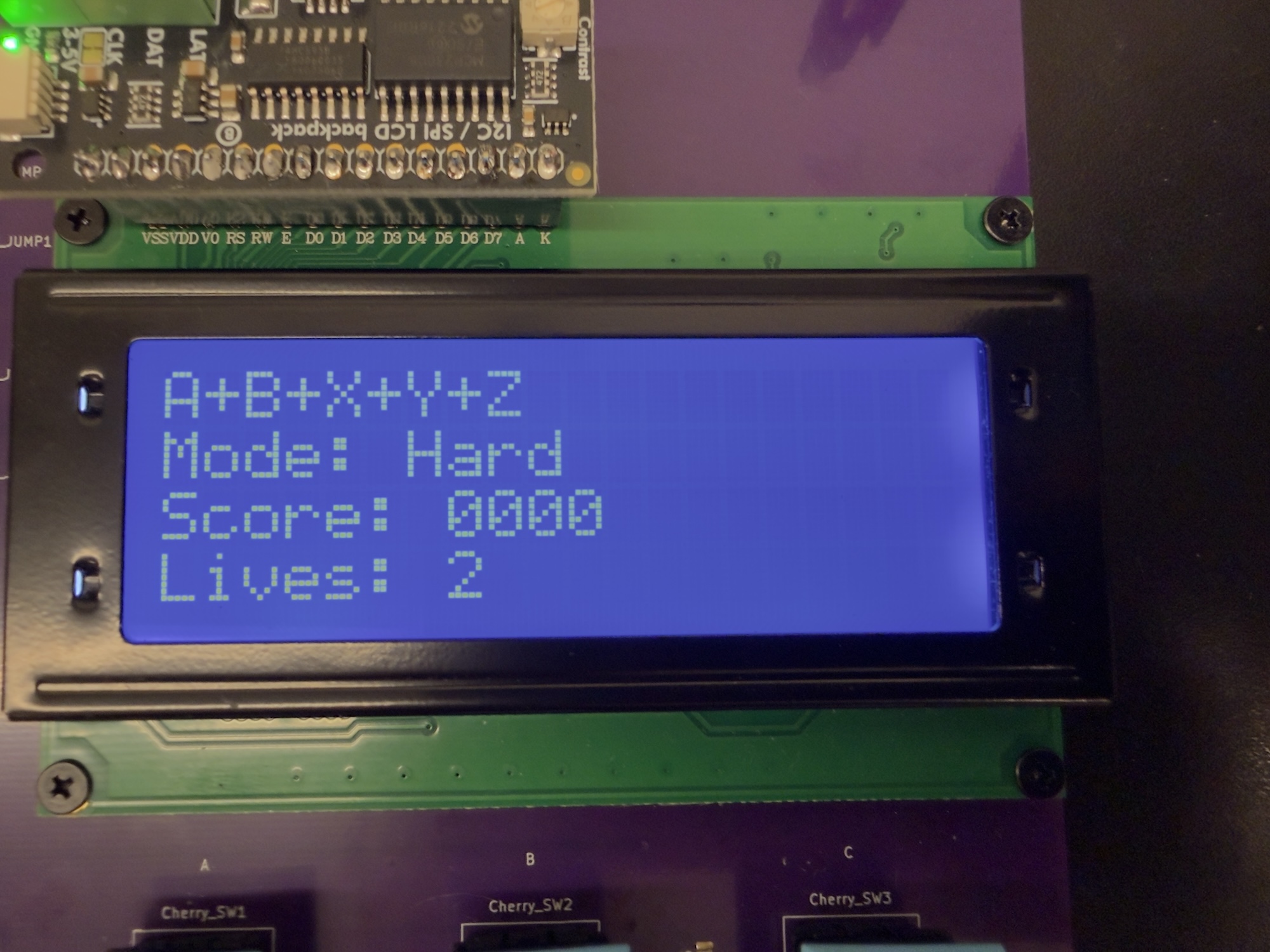
Game Hard Mode In Progress
Video Demonstration
Chip Specifications
| Parameter | Specification |
|---|---|
| Technology | TSMC 65nm GP |
| Die Size | 2.0mm × 1.0mm |
| Maximum Frequency | 200 MHz |
| Operating Frequency | 84.414 MHz |
| Supply Voltage | 1.0 V core rails (VDD_CORE / VDD_CLEAN / VDD_TEST), 3.3 V I/O, 5 V board input |
| Power Consumption | 2.151 mW typical |
| Package | LQFP64L |
| Gate Count | ~450,000 gates |
The table below defines the memory map of all major components connected to the SoC bus. Each peripheral is assigned a dedicated, non-overlapping address region to ensure simple decoding and deterministic access behavior. The on-chip data memory (DMEM) occupies the lower address space, enabling fast load/store operations from the CPU core. All memory-mapped peripherals—including GPIO, UART, SPI, I²C, and timer modules—are placed at aligned 4 KiB address boundaries on the bus. This organization allows the AHB/APB interconnect to efficiently route transactions based on the high-order address bits, while providing a clean, extensible structure for integrating additional peripherals in future revisions of the SoC. The CPU can interact with each module through standard load/store instructions, making software development straightforward and enabling uniform access across the entire system.
| Device | Start | End | Size |
|---|---|---|---|
| DMEM | 0x00000000 | 0x00007FFF | 16KiB |
| GPIO | 0x10000000 | 0x10000FFF | 4KiB |
| UART | 0x20000000 | 0x20000FFF | 4KiB |
| SPI | 0x30000000 | 0x30000FFF | 4KiB |
| I²C | 0x40000000 | 0x40000FFF | 4KiB |
| Timers | 0x50000000 | 0x50000FFF | 4KiB |
In addition to the bus-mapped peripheral address space, the SoC includes a separate memory map for the instruction memory (IMEM). Unlike DMEM and the peripheral modules, IMEM is not connected to the AHB/APB system bus. A separate IMEM table is therefore provided to document its address boundaries and organization.
| Device | Start | End | Size |
|---|---|---|---|
| IMEM | 0x00000000 | 0x00007FFF | 16KiB |
The table below summarizes the output frequencies generated by the on-chip clock generator for different combinations of clkgen_div and clkgen_fc control signals. These configuration bits are loaded through the scan chain, allowing the clock generator to be fully programmable without requiring dedicated external pins. By shifting the desired divider (clkgen_div) and frequency-control (clkgen_fc) values into the scan chain and applying them during run mode, the SoC can dynamically select a wide range of operating frequencies. This programmability enables flexible performance scaling, thorough post-silicon characterization, and simplified validation of timing margins across various clock settings.
| clkgen_div | clkgen_fc | Frequency (Hz) |
|---|---|---|
| 1111 | 11111 | 9.3424K |
| 1111 | 01010 | 20.682K |
| 1111 | 00101 | 29.361K |
| 1110 | 01010 | 41.358K |
| 1110 | 00101 | 58.685K |
| 1101 | 01010 | 82.672K |
| 1101 | 00101 | 117.35K |
| 1100 | 01010 | 165.43K |
| 1100 | 00101 | 234.80K |
| 1011 | 01010 | 330.69K |
| 1011 | 00101 | 468.87K |
| 1010 | 01010 | 661.38K |
| 1010 | 00101 | 938.44K |
| 1001 | 01010 | 1.321M |
| 1001 | 00101 | 1.877M |
| 1000 | 01010 | 2.637M |
| 1000 | 00101 | 3.765M |
| 0111 | 01010 | 5.252M |
| 0111 | 00101 | 7.530M |
| 0110 | 01010 | 10.593M |
| 0110 | 00101 | 15.010M |
| 0101 | 01010 | 21.552M |
| 0101 | 00101 | 30.02M |
| 0100 | 01010 | 42.264M |
| 0100 | 00101 | 59.98M |
| 0011 | 01010 | 84.414M |
| 0011 | 00101 | 119.66M |
| 0010 | 01010 | 168.83M |
| 0010 | 00101 | 239.46M |
| 0001 | 01010 | 336.75M |
| 0001 | 00101 | 476.74M |
| 0000 | 01010 | 669.16M |
| 0000 | 00101 | 946.97M |
| 0000 | 00000 | 1.524G |
Conclusions
Key Achievements
Our team successfully designed and verified a fully functional RISC-V-based System-on-Chip (SoC) integrating a custom CPU core, AHB/APB bus interconnect, instruction and data memories, and a rich set of peripheral modules including UART, SPI, I²C, GPIO, LCD, timers, finite-state machines, and a full scan chain architecture. We implemented a complete end-to-end ASIC design flow, from architectural design, RTL implementation, and verification to synthesis, physical design, and tape-out, resolving all timing violations and achieving clean DRC/LVS signoff. To support software development, we built a customized RISC-V toolchain, linker script, and utilities tailored for a Harvard memory architecture. A comprehensive test suite, covering arithmetic kernels, peripheral interactions, metastability tests, and multiple demonstration programs, was developed and validated across both RTL and post-synthesis gate-level simulations. We also integrated deterministic scan-chain–based loading and run-mode execution for robust software-driven testing. Full post-route timing analysis and signoff were completed using Innovus, Virtuoso, and PrimeTime, culminating in the generation of the final GDSII and all required collateral for fabrication. After silicon returned, we performed post-silicon validation, designed a custom PCB for bring-up, and developed multiple demo applications to showcase the chip’s full functionality running on real hardware.
Lessons Learned
Throughout the design and implementation of the SoC, we gained several important insights that shaped our engineering workflow. Managing a hierarchical SoC design requires careful planning of module interfaces, timing constraints, and verification strategies to ensure smooth integration and to prevent late-stage system-level issues. We found that addressing toolchain setup, linker configuration, and memory mapping early in the project greatly simplified software debugging and hardware bring-up. From a physical design standpoint, we learned that hold-time violations frequently emerge after synthesis and must be handled systematically during place-and-route through delay insertion and routing optimization. Additionally, macro placement, power grid design, and clock tree architecture proved to have substantial impact on timing closure, congestion, and overall chip robustness. Building a comprehensive testing framework—including both RTL and gate-level simulations—was essential to uncovering subtle timing and functional issues long before tape-out.
After tape-out, we further learned the importance of planning for post-silicon validation, including designing accessible scan-chain hooks, preparing diagnostic firmware, and building modular test infrastructure. The bring-up process highlighted the value of well-organized PCB design, clear pin documentation, and flexible debugging utilities to quickly isolate hardware or software faults. Finally, developing real demo applications on the fabricated chip reinforced the need for strong coordination between hardware, firmware, and system validation, demonstrating that successful silicon requires not only correct design, but also thoughtful preparation for real-world testing and integration.
Future Work
Looking ahead, several enhancements could significantly elevate the capability and performance of the next-generation SoC. CPU performance can be further improved through enabling the FPU or switching to a more performant CPU design. On the system level, integrating advanced peripherals such as DMA controllers, interrupt subsystems, or dedicated hardware accelerators for graphics or AI workloads would greatly expand the chip’s versatility. Power efficiency could be improved by introducing power-domain partitioning, fine-grained clock gating, and other low-power design techniques. From a tooling perspective, extending the software toolchain to support richer debugging features such as on-chip breakpoints, real-time trace modules, or a full JTAG interface would streamline firmware development and hardware bring-up. For physical design scalability, migrating to a more advanced technology node or increasing metal-layer count would enable higher operating frequencies and denser integration. Ultimately, these improvements could contribute to a second-generation SoC featuring larger on-chip memory, higher-speed interfaces, and greater interconnect bandwidth to support more complex real-world applications.
References
- OpenHW Group. CV32E40P User Manual. docs.openhwgroup.org
- ARM Ltd. AMBA APB Protocol Specification (IHI0033). developer.arm.com
- ARM Ltd. AMBA AHB Protocol Specification (IHI0011). developer.arm.com
- iRisc Team. iRisc: Fully Custom RISC-V SoC (2024). gitfront.io
- RISC-V Collaboration. RISC-V GNU Toolchain. github.com/riscv-collab/riscv-gnu-toolchain
- OpenHW Group. CV32E40P RISC-V CPU. github.com/openhwgroup/cv32e40p
- Pulp-Platform. APB_SPI_Master. github.com/pulp-platform/apb_spi_master
- Pulp-Platform. APB_UART. github.com/pulp-platform/apb_uart_sv
- Pulp-Platform. APB_I2C. github.com/pulp-platform/apb_i2c
- Pulp-Platform. APB_GPIO. github.com/pulp-platform/apb_gpio
- Pulp-Platform. APB_Timer. github.com/pulp-platform/apb_timer
Acknowledgments
We would like to express our deepest gratitude to Professor Mingoo Seok, whose weekly meetings, technical guidance, and continuous encouragement were fundamental to the success of this tape-out project. His insights into this area helped shape our SoC from concept to working silicon, and his support throughout each milestone kept our team moving forward.
We would also like to thank our teaching assistants for their invaluable contributions. Da Won Kim’s lessons provided essential foundational knowledge that directly strengthened our design flow work. Mosom Jana’s office hours were instrumental in helping us resolve numerous technical challenges, from RTL implementation to back-end design issues. We are grateful to Chuan-Tung Lin for his extensive support during silicon validation, PCB development, and the final demo; his guidance played a critical role in enabling our successful bring-up and demonstration of the fabricated chip.
We further acknowledge the EE6350 VLSI Design Lab 2024 RISC-V Processor Team, whose previous work served as an important reference as we built our own system. We extend our appreciation to James Tian, whose timely assistance and practical advice helped us overcome difficulties throughout the project. We are also thankful for the collaboration and discussions with students from other fellow groups, the shared problem-solving environment in the lab greatly enriched our learning experience and contributed to the overall success of the project.
Finally, we would like to extend our sincere appreciation to Apple Inc. for sponsoring this tape-out project. We are especially grateful to the Apple engineers whose guidance, technical insights, and continuous support played an essential role in helping us improve our design and better understand real-world ASIC development practices. Their contributions greatly enriched our learning experience and enabled us to complete this project successfully from design through silicon validation.