Introduction
Welcome to the SoC team page! We present a complete RISC-V System-on-Chip (SoC) implemented and
taped out in TSMC 65-nm technology. This work was developed as part of Columbia University’s
EE6350 VLSI Laboratory, and we gratefully acknowledge the supervision of Prof. Mingoo Seok,
the generous support from Apple Inc., and the support of the course TAs.
The chip adopts a CPU–VPU heterogeneous architecture, integrating the open-source PicoRV32 RISC-V
CPU and a custom-designed VPU, along with on-chip memory and essential I/O (UART, SPI), to
accelerate data-parallel workloads such as vector operations and convolution-like kernels used in
image processing and lightweight AI pipelines. The CPU provides system-level programmability and
orchestration, while the VPU couples a SIMD datapath with a dedicated control plane for vector
decode, memory sequencing, and PE scheduling. This separation enables straightforward CPU-only vs.
VPU-offloaded benchmarking, making acceleration benefits easy to reproduce and quantify on silicon.
From RTL design and verification through synthesis, place-and-route, and pad integration, we
completed an end-to-end ASIC flow and validated the chip via post-silicon board bring-up and
testing. The result is a compact, software-programmable platform that demonstrates digital system
integration and silicon-proven hardware/software co-design.
System Architecture
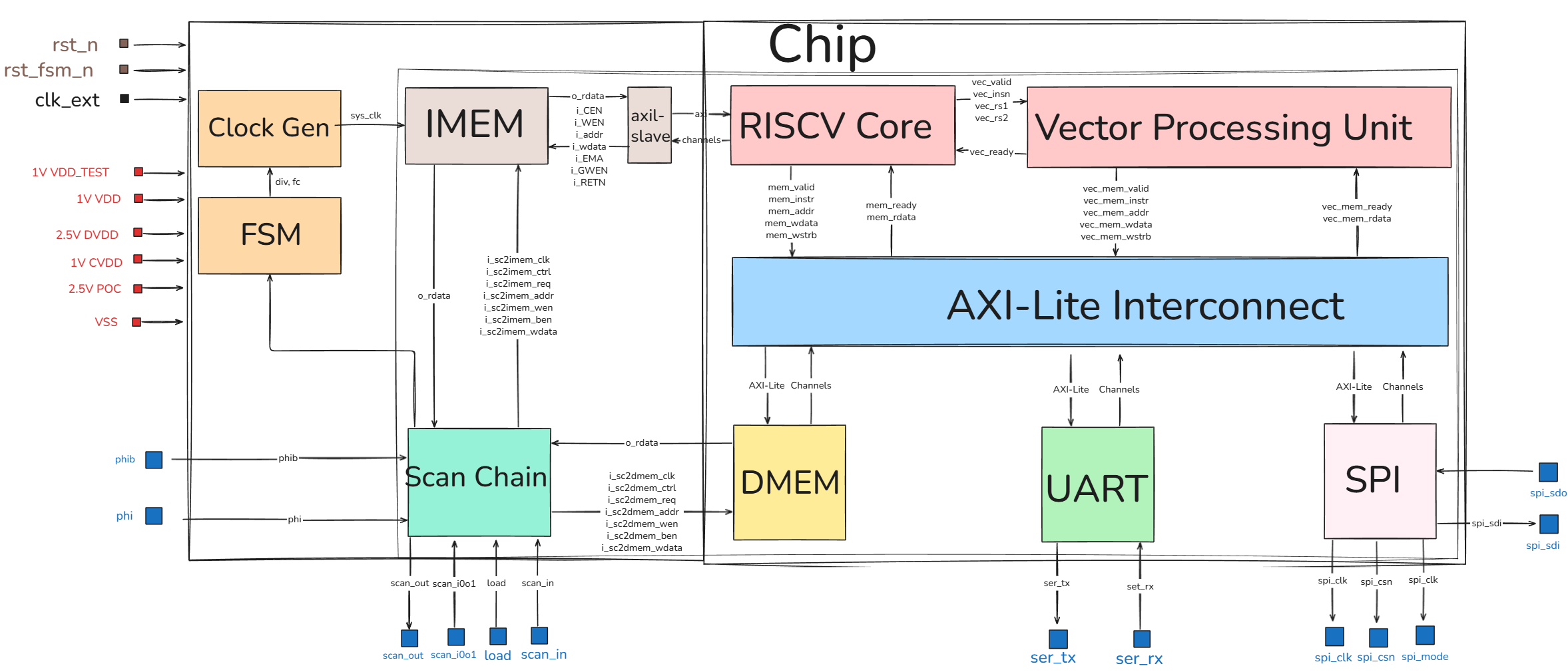
This diagram illustrates the architecture of our RISC-V based System-on-Chip (SoC). At its core, a RISC-V processor is paired with a dedicated Vector Processing Unit to handle accelerated parallel computations. These processing units communicate with system resources via a central AXI-Lite Interconnect. Essential external communication is handled through UART and SPI interfaces. Additionally, the design incorporates support infrastructure, including a Clock Generator, Finite State Machine (FSM), and a Scan Chain for hardware testing and debugging.
Key Modules
Vector Processing Unit (VPU)
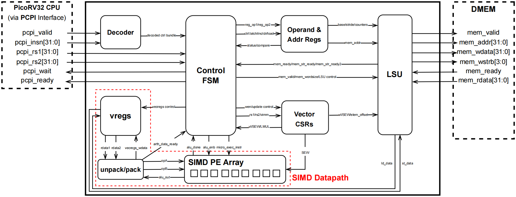
This custom VPU is a PCPI-attached accelerator for PicoRV32 that delivers silicon-proven speedup on data-parallel kernels while keeping the CPU microarchitecture unchanged. It integrates a dedicated control plane (instruction decode + multi-cycle control FSM) that autonomously manages instruction sequencing, base/stride address generation, memory handshaking, and PE scheduling, so the CPU simply issues an offload and waits for completion via pcpi_wait/pcpi_ready. Vector state is maintained in small control registers (e.g., vl and vtype), from which SEW/LMUL are derived to parameterize datapath packing and memory behavior. Operands/results are stored in a 288-bit vector register file, with an unpack/pack stage feeding a 9-lane SIMD PE array for element-wise compute (e.g., vector multiply) matched to the register packing granularity. For data movement, a vector load/store subsystem converts each vector memory instruction into a tightly sequenced stream of back-to-back 32-bit DMEM transfers, moving up to nine 32-bit lanes per vector and eliminating scalar loop/address-update overhead. This hardware-sequenced, aggregated access pattern reduces per-transaction overhead and helps sustain throughput on a 32-bit, non-burst memory interface, making the design especially effective for convolution- and MAC-heavy workloads and enabling clean, reproducible CPU-only vs. CPU+VPU benchmarking under the same workload code. Across our measured demos, end-to-end speedup increases monotonically with VPU utilization (vector intensity), ranging from ~1× at low utilization up to ~6× at high utilization. As a result, the SoC is particularly well-suited for CNN-style AI kernels—where the inner loops are dominated by vectorizable multiply–accumulate (MAC) patterns and regular tensor-like memory access—so this design can be viewed as a compact, AI-oriented accelerator chip for convolutional workloads.
For technical details on the VPU, reach out to Jiajun Jiang.
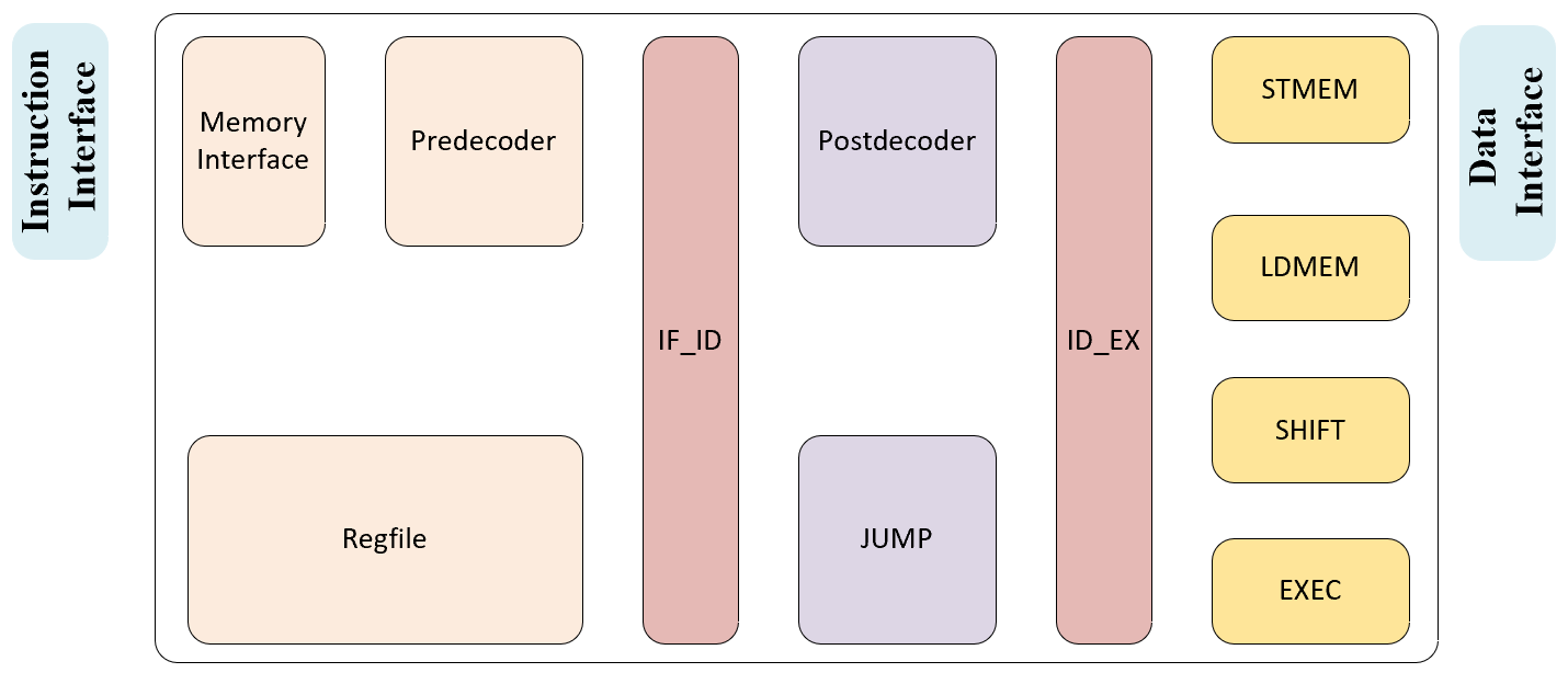
CPU Core: picorv32
The system is anchored by the PicoRV32, a robust and widely adopted open-source
RISC-V CPU core designed for high reliability and area efficiency.
It implements the standard RISC-V RV32I Instruction Set Architecture (ISA),
providing a comprehensive suite of base integer instructions.
Architecturally, the PicoRV32 is engineered with a focus on timing closure;
its design minimizes logic depth in the critical path, allowing the core to
achieve a high maximum operating frequency 270MHz in TSMC65nm even in area-constrained
layouts. Crucially, the core features a dedicated Pico Co-Processor Interface (PCPI).
This low-latency interface serves as the bridge to our custom Vector Processing Unit (VPU),
allowing the PicoRV32 to seamlessly offload complex vector instructions
while maintaining rigorous control over system flow and data consistency. Below Shows the Finite State Machine of this simple RISCV Core.
Bus Interconnect: AXI-Lite Interconnect
The open-source AXI-Lite Interconnect we adopted supports multiple masters and slaves. The maximum frequency after synthesizing is around 500 MHz and the area is pretty small. It does not support burst transactions, out-of-order (OoO), or outstanding transactions in the AXI protocol.
System Memory Map
| Device / Region | Start Address | End Address | Size |
|---|---|---|---|
| Instruction Memory (IMEM) | 0x0000_0000 |
0x0000_7FFF |
32 KB (0x8000) |
| Data Memory (DMEM) | 0x0000_8000 |
0x0000_FFFF |
32 KB (0x8000) |
| UART | 0x0010_0000 |
0x0010_000F |
16 Bytes (0x10) |
| SPI | 0x0010_0000 |
0x0010_00A3 |
164 Bytes (0xA4) |
Memory Subsystem: IMEM & DMEM
To maximize on-chip storage efficiency, the SoC integrates 64KB of SRAM, symmetrically divided into 32KB for Instruction Memory (IMEM) and 32KB for Data Memory (DMEM). We utilized the ARM Artisan Memory Compiler to generate these high-density, single-port memory macros. To ensure seamless connectivity, custom wrappers were developed to bridge the memory interface with the processor core. Furthermore, these wrappers facilitate system initialization, allowing instructions and data to be pre-loaded directly through the scan chain.
I/O Peripherals: UART & SPI
UART (Host + Display Bridge for Demo)
The SoC provides a UART interface used as the main link for bring-up, control, and demo I/O. In the demo setup, a PC communicates with the chip through an ESP32-DevKitC-32E, which serves as a compact USB-to-UART bridge and controller. A TXS0108E 8-channel level shifter is used to translate logic levels between the chip I/O domain and the 3.3 V external hardware. Through this UART path, the host can trigger workloads, read back status/cycle counters, and stream result data. The same UART link also enables visualization on a 240×240 IPS LCD module via the external controller, allowing processed images and intermediate results to be displayed in real time during demonstrations.
SPI (External Storage / Parameter Expansion Interface)
The SoC exposes an SPI interface as an external storage expansion port, designed for use cases where model parameters, lookup tables, or large input tensors exceed on-chip memory capacity. In a typical workflow, the chip can pull blocks of data over SPI into on-chip DMEM before launching compute, enabling re-parameterization (e.g., swapping CNN weights or coefficients) without rebuilding the entire on-chip image. This is a practical and widely used design point for compact accelerators: SPI provides a simple, pin-efficient, and board-friendly path to attach off-chip memory or a storage controller. For prototyping and demos, the SPI target can be implemented flexibly—an FPGA can emulate external memory behavior, or the interface can connect to other off-chip storage solutions—providing a scalable route toward larger AI workloads while keeping the on-chip design lightweight.
DFT Module: Scan Chain, Clock Generator, Testing FSM
Our chip uses a custom, academic-level DFT infrastructure whose central element is a scan chain, together with the on-chip clock generator and the mode-control FSM. These modules enable post-silicon functional testing by providing a unified method to load programs/data into on-chip memories and configuration registers, and to read internal state back out of the fabricated chip.
Scan Chain
The scan chain contains 252 scan cells connected between the external pins scan_in and scan_out.
Each cell corresponds to one bit of internal state, including instruction/data memory address and data buses, as well as
configuration registers for the clock generator and the testing FSM. In normal operation, memories are driven by the core,
but in test mode the scan chain can temporarily take over—driving/sampling these ports and enabling readback of memory contents
to verify correct execution.
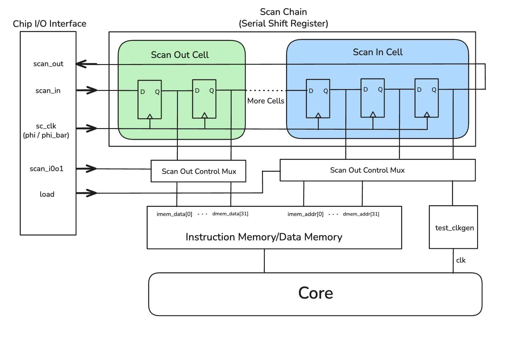
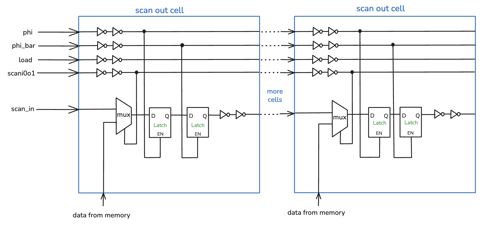
The figures below illustrate the internal structure of the scan cells and their connection in the chain. A control signal
scan_i0o1 selects the operating mode. Internally, scan-in and scan-out cells use an input-select MUX and two
back-to-back transparent latches clocked by non-overlapping scan clocks, which helps avoid hold-time issues common in long shift registers.
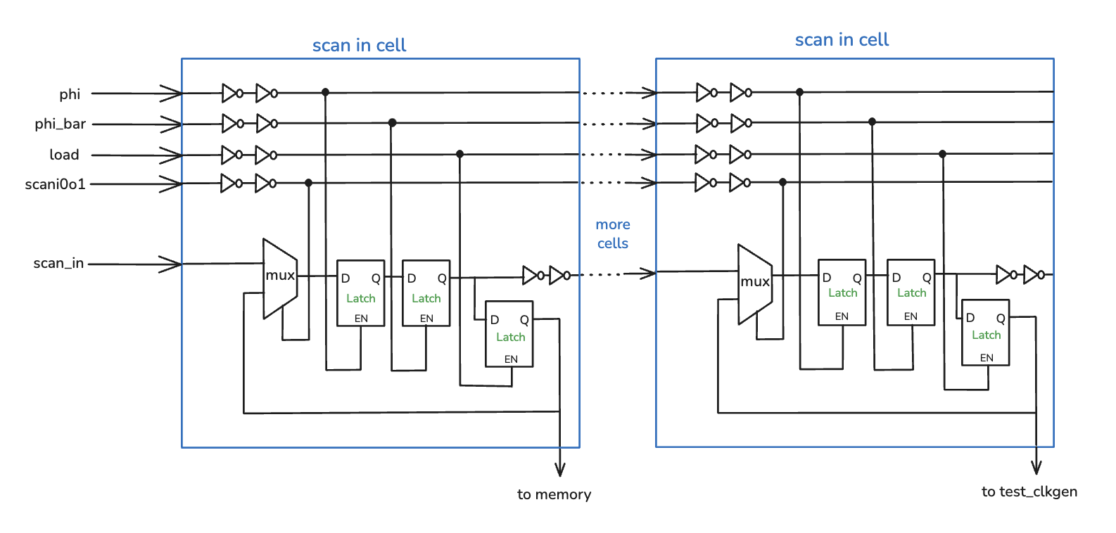
During testing, we stream a serial bit pattern into scan_in while toggling the scan clock. After 252 shift cycles,
the pattern propagates to all cells. When scan_i0o1 is configured for scan-in and the load signal is pulsed, the scan
contents are written into connected memories and control registers (e.g., instruction address/data, clock generator settings
div/fc/en_int, and FSM mode/cycle count). Some scan cells also provide “virtual” memory clocks
imem_clk/dmem_clk; we emulate a rising edge by re-loading the same scan pattern with that clock bit toggled from low to high.
Readback is symmetric: with scan_i0o1 set to scan-out, selected memory/register signals feed the scan-out cells. After latching,
we shift out the 252-bit vector through scan_out, enabling inspection of internal state and dumping results from DMEM using the same interface.
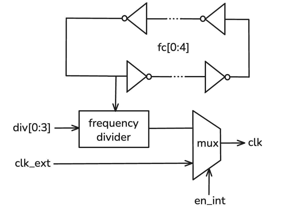
Clock Generator
To support flexible post-silicon testing and controlled operating frequencies, our SoC includes a programmable on-chip clock generator.
Its control signals are loaded through the scan chain: fc[0:4] provides fine tuning by adjusting oscillator length, and
div[0:3] sets a coarse digital divide ratio. A chip I/O signal en_int selects between the internal clock path and an
external reference clock clk_ext. Together these controls generate the system clock clk with selectable frequency and source.
Testing FSM
For controlled post-silicon debugging, we added a small finite-state machine (FSM) that drives clock-gating logic. All FSM mode controls
are loaded through the scan chain. During scan shift operations, the FSM holds the system clock off to prevent unintended state changes.
In run mode, it propagates the selected clock source (internal or external) to the SoC. In countdown mode, it enables the clock for a
programmed number of cycles and then turns it off, allowing cycle-accurate inspection of internal state.
Design Flow
The following diagram outlines the complete RTL-to-GDSII design flow implemented for this project. It highlights the transition from behavioral Verilog RTL through Synthesis and Place & Route, utilizing industry-standard tools for verification at every stage.
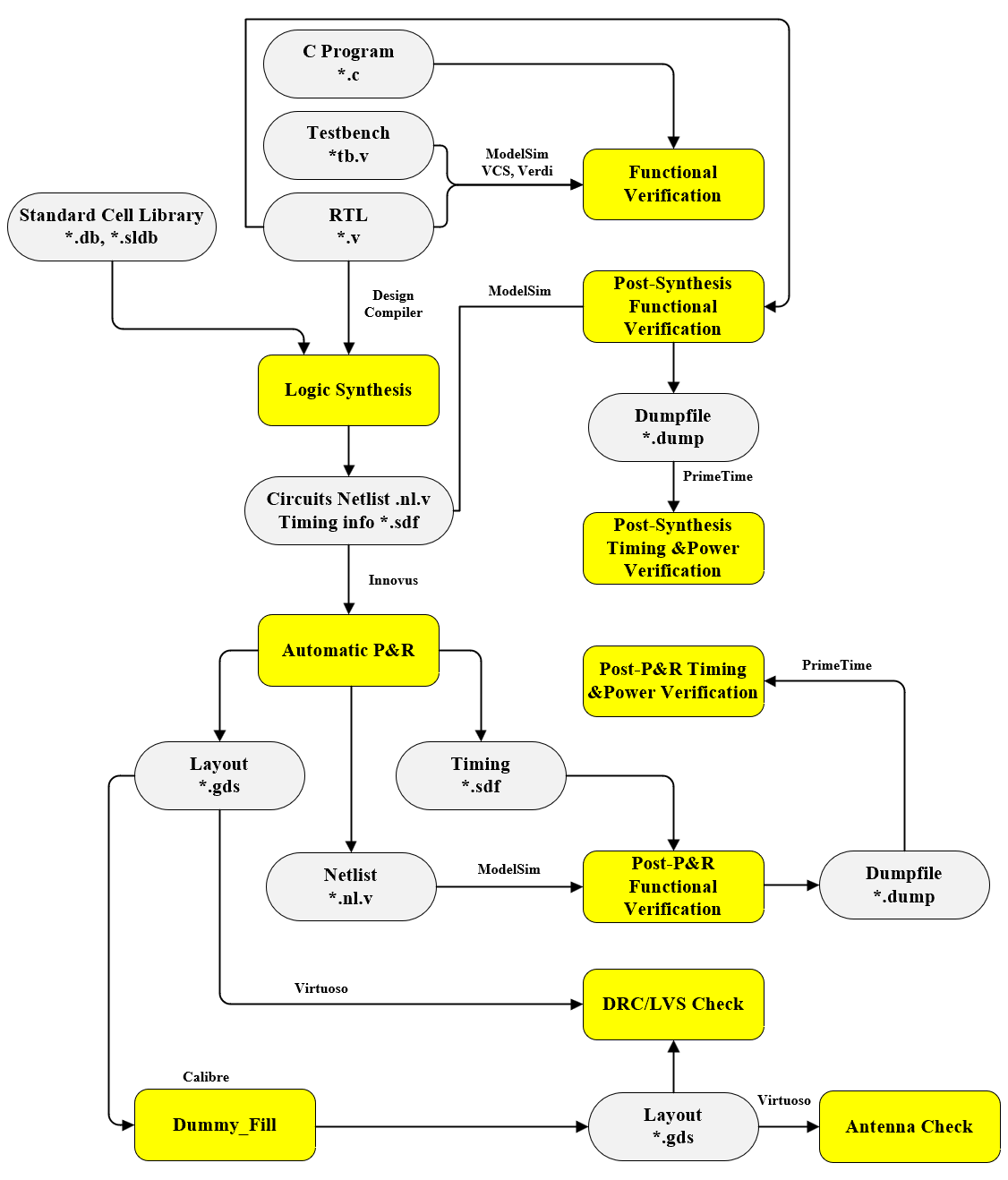
RTL Design
The RTL (Register Transfer Level) design serves as the core of our digital implementation, bridging the gap between high-level algorithms and physical hardware.
Hierarchical Design & Verification
We adopted a rigorous Bottom-Up Implementation strategy. Design work starts with coding individual, low-level submodules. Once these leaf blocks are completed, they are integrated into larger parent modules, eventually culminating in the Top-Level SoC.
Verification follows a corresponding layered approach:
- Unit-Level Verification: Submodules are first verified in isolation using dedicated testbenches to ensure local correctness.
- Integration Verification: As blocks are assembled, verification focuses on interface protocols and data flow between modules.
- Full-Chip Verification: The complete design is simulated (using tools like ModelSim, VCS, and Verdi) and cross-compared against the C reference model to validate system-wide functionality.
| Version | Feature |
|---|---|
| 0.0 | Basic Model from PicoRV32 RISCV Core |
| 0.1 | Integrated Instruction SRAM with memory wrappers |
| 0.2 | Integrated AXI-Lite Interconnect |
| 0.3 | Integrated Data SRAM with memory wrappers |
| 0.4 | Integrated Scan Chain |
| 0.5 | Integrated UART and SPI |
| 0.6 | Integrated Vector Processing Unit |
| 0.7 | Integrated Clock Generator, Scan Chain and FSM |
| 0.8 | Modified Vector Processing Unit for Smaller Size |
| 0.9 | Integrated Pad Frame and IO Cells |
| 1.0 | Verified Functionality from Chip Level and RTL Freeze |
Synthesis
We used Synopsys Design Compiler for logic synthesis. Before running synthesis, we prepared a complete SDC file that defined all necessary constraints, including clock definitions, clock constraints, drive and load constraints, operating conditions, and wire-load models. Specifically, the SDC file included parameters such as clock name, clock period, clock uncertainty, clock transition, as well as input and output delay constraints. Our chosen synthesis strategy followed a bottom-to-top approach. We first synthesized several major submodules independently, such as the CPU core and the VPU module. The remaining modules were synthesized together within the top-level design, while the pre-synthesized blocks were marked as don't touch to preserve their optimized structures. This process allowed us to generate the complete set of netlist files for the entire chip.
Physical Design
Auto P&R
We used Cadence Innovus for our physical design. In our place-and-route flow, the major steps included:
loading design files, floorplanning, power routing, cell placement, pre-CTS optimization, clock tree synthesis (CTS),
signal routing, RC parasitic extraction, filler cell insertion, design verification, and final GDS files output.
The physical hierarchy of the chip consists of submodules, the top module, the chip-level module, and the IO pads.
Our place-and-route strategy followed the same bottom-up approach used during synthesis. The Dmem and Imem blocks used
existing layout macros, while modules such as the SPI block, scan chain, test FSM, coprocessor, and CPU core were placed
and routed independently. The remaining modules were integrated and routed within the top-level design.
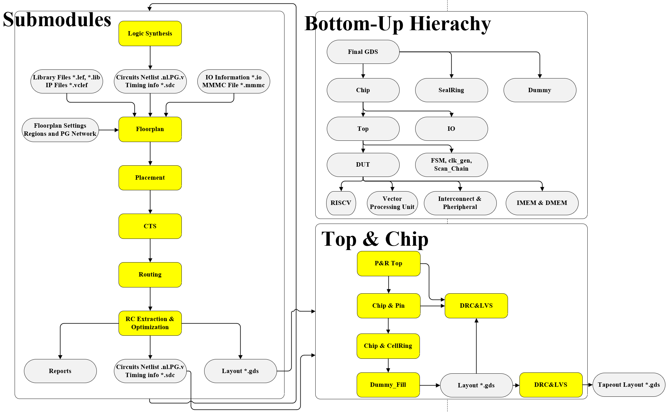
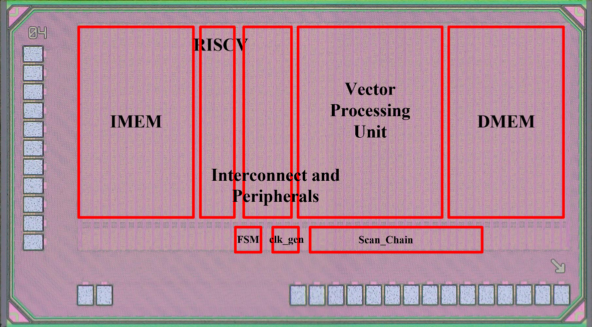
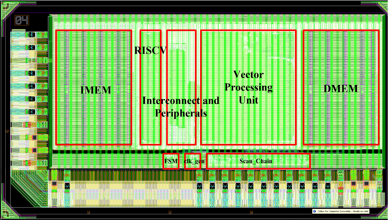
The final result is the complete chip-level layout, as shown in the figure. The two memory blocks are placed on opposite ends of the layout, while the central region contains key macros such as the CPU core and the VPU. The scan chain and clock generator are positioned toward the outer region but kept as close as possible to the center to minimize clock skew. Surrounding the entire design are the required IO pads that interface the chip with the external system.
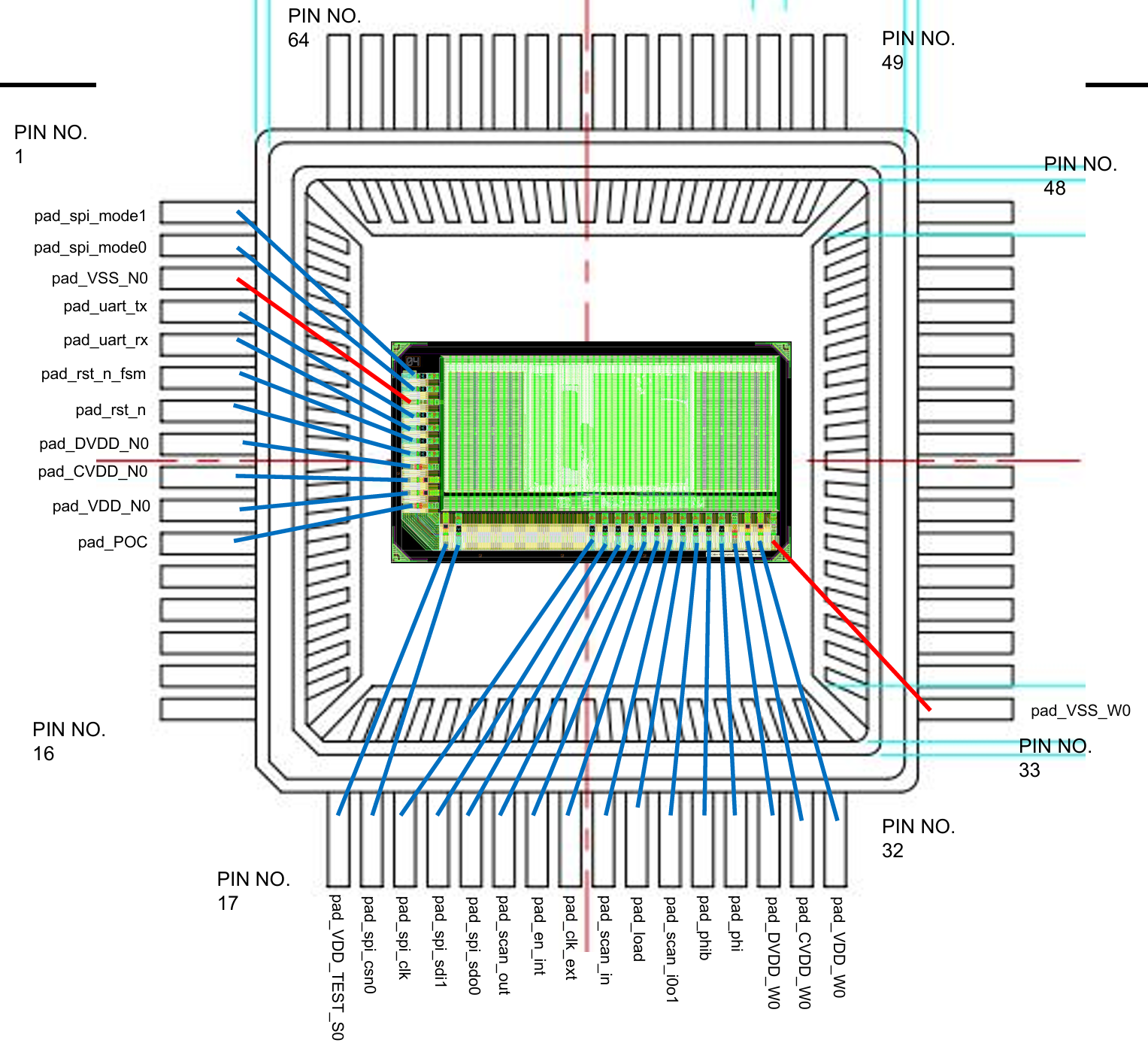
IO Pad
Below shows the IO Pad integration based on LQFP64L: We have 11 + 16 + 1 = 28 IOs.
These IOs include input/output signals (SPI, UART, Scan_Chain, rst_n, clk), POC,
CVDD, DVDD, VDD, VDD_TEST, and GND. We tried to minimize our IO number because we need a bigger area for logic circuits.
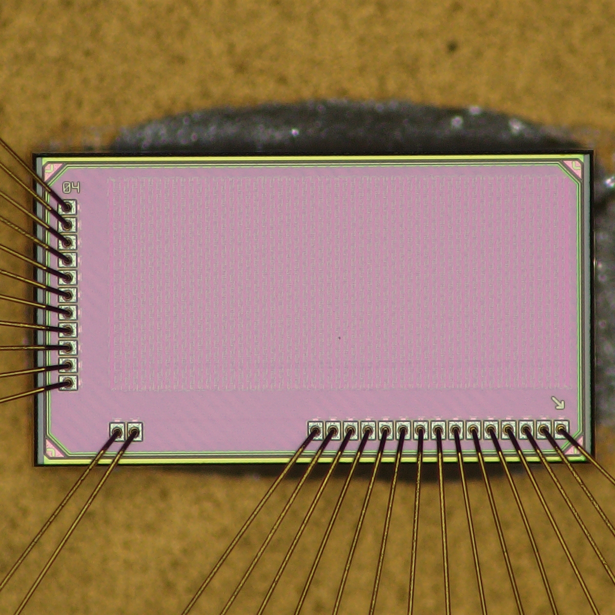
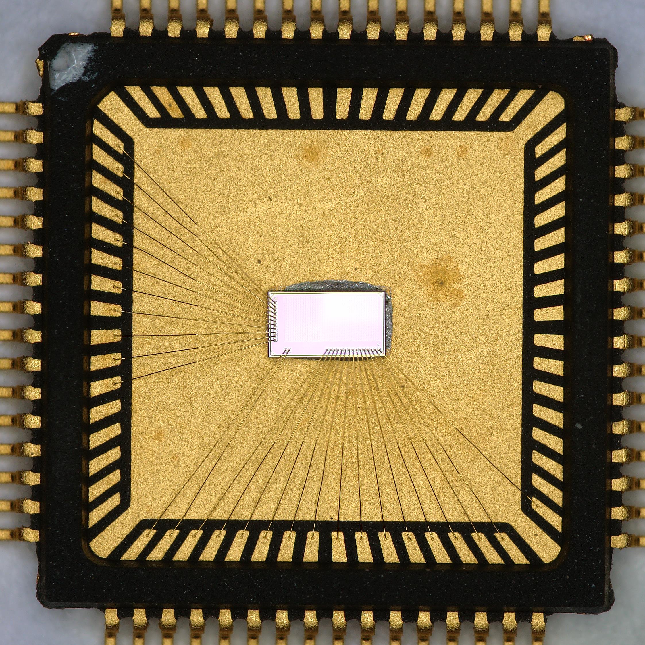
Package
Below is the picture of our taped out chip with bonding wires and packages.
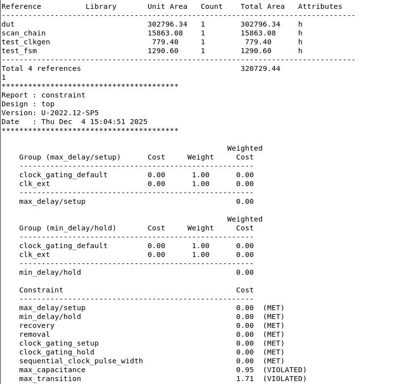
STA & Sign-off
During the STA phase, we used PrimeTime with a target operating frequency of 100 MHz. After place-and-route, the clock uncertainty was controlled within approximately 0.5 ns. According to the timing reports, all critical paths within the top module met their setup and hold time requirements, and no setup or hold violations were observed. In addition, the asynchronous reset signals passed all recovery and removal checks without violations.
After completing the physical design, we performed full signoff verification on each submodule and the top-level design. Using Mentor Calibre, we conducted DRC, LVS, ESD, and antenna rule checks to ensure that all results were clean. Only after passing all signoff criteria did we proceed with the final GDS files export of our chip.
PPA Optimization
In our chip design, we placed strong emphasis on PPA (Power, Performance, Area) optimization. Several low-power techniques were applied throughout the design stages:
- Fixed Voltage Domains: The chip uses fixed voltage domains, with 2.5V for IO pads and 1.0V for the core logic, ensuring stable and efficient power distribution.
- Clock Division: We applied clock division techniques. For example, the SPI module operates on a divided clock derived from the main clock, reducing switching activity and lowering dynamic power consumption.
- RTL Resource Sharing: At the RTL level, we adopted resource sharing, reusing registers and functional units whenever possible to reduce redundant hardware.
- State Encoding Optimizations: State encoding optimizations were applied, such as using Gray code instead of conventional binary encoding to minimize bit toggles and reduce dynamic power.
- Automatic Clock Gating: During synthesis, automatic clock gating was enabled to shut off clocks when modules are idle. Although this increases area slightly, it significantly reduces dynamic power consumption.
- High-Vth Cell Insertion: In the physical design stage, we selectively replaced LVT (Low-Vth) cells with HVT (High-Vth) cells, which reduces leakage power at the cost of some performance and area overhead.
These combined strategies allowed us to effectively manage power while maintaining overall performance and design efficiency.
Software & Testing Flow
The software and testing flow converts C-level test programs into memory-mapped initialization data, generates scan sequences, and loads them onto silicon through an FPGA-based scan controller. This unified environment supports both pre-silicon verification and post-silicon validation of the CPU, memory system, and VPU.
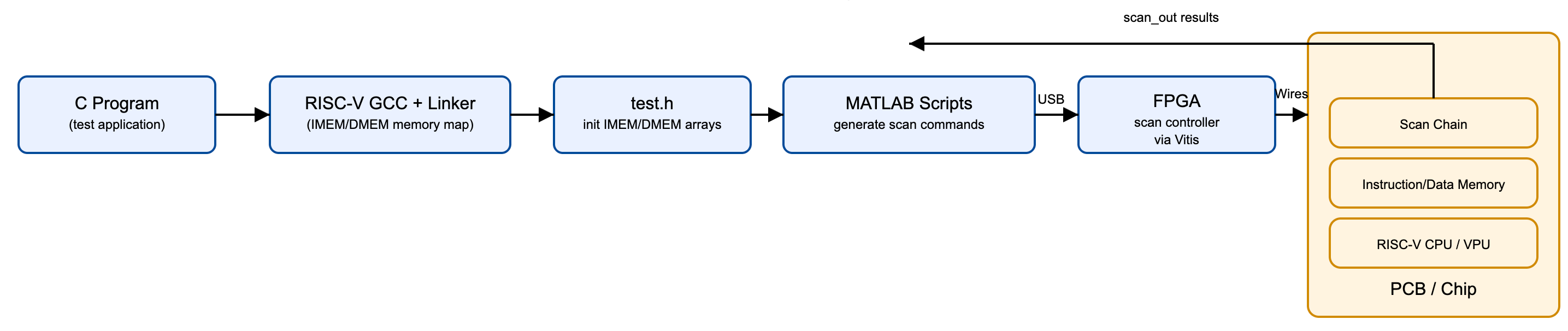
Software Development
Test applications are written in C and compiled using a customized RISC-V GCC toolchain
aligned with the chip's IMEM/DMEM memory map. The linker output is automatically
converted into test.h, which contains the initialization arrays for
instruction and data memory. These files form the common interface between software
and the scan-based testing environment.
The software framework allows different test programs to be executed on silicon, including routines that stress the CPU pipeline, memory system, or vector/AI units. Inline RISC-V assembly is supported for low-level testing of microarchitectural features.
Testing Methodology
MATLAB scripts serialize the IMEM/DMEM initialization arrays into cycle-accurate
scan-in command sequences. These command streams are transferred to an FPGA board
over USB, where a Vitis-based scan controller shifts data into the chip’s scan chain.
After execution, the FPGA retrieves scan_out data for functional
comparison and validation.
PCB Design
We used a PCB board for our final demonstration. The PCB helps provide power, voltage stabilization, and decoupling.
Schematic
The schematic of the PCB layouts mainly includes three parts: main circuits, power supply circuit, and decoupling circuits.
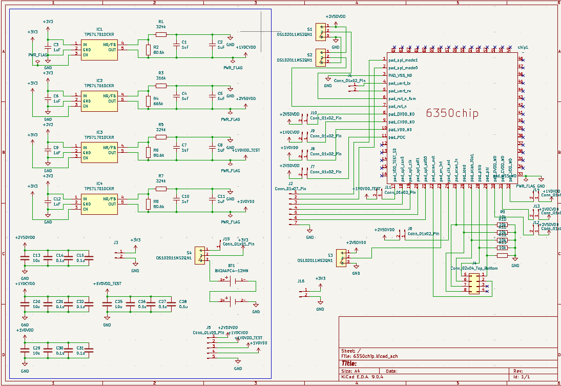
In the main circuits, we created the symbol for our chip. The footprint of our chip is LQFP-64 (10×10 mm, 0.5 mm pitch). Some pins are not used. Reset IO pins are connected to switches, so we can control reset to VDD/GND by hand (asynchronous reset). DVDD powers IO pads, and VDD powers the core. All resistors and capacitors use 1206 footprints. The PCB supports two power modes (battery or FPGA), selectable by a switch.
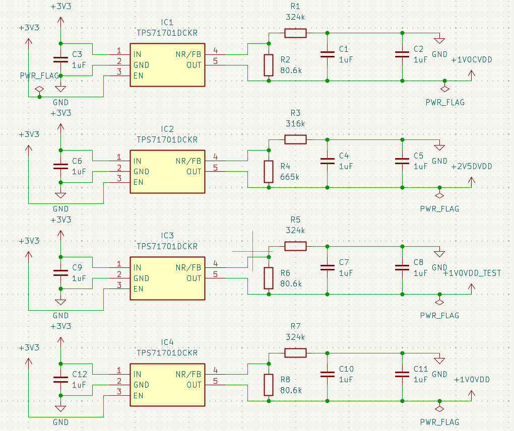
In the power supply circuit, the LDO transfers 5V to 2.5V and 1V. The resistor and capacitor values for input/output filtering follow the TI reference recommendations for TPS71710CDR.
The decoupling circuit is designed to reduce supply noise during operation. The number of capacitors is determined by the requirements of each power net.
The main circuit connects the chip to other board components. We used jumpers for debugging and left pins for FPGA connections. The PCB was manufactured by JLCPCB, and soldering was performed manually.
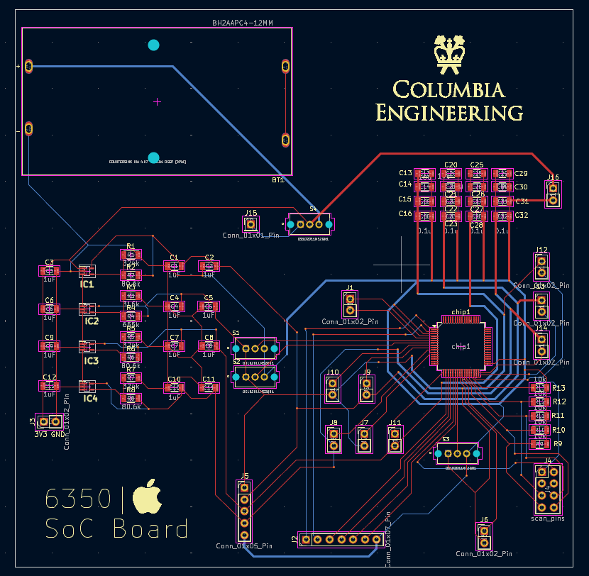
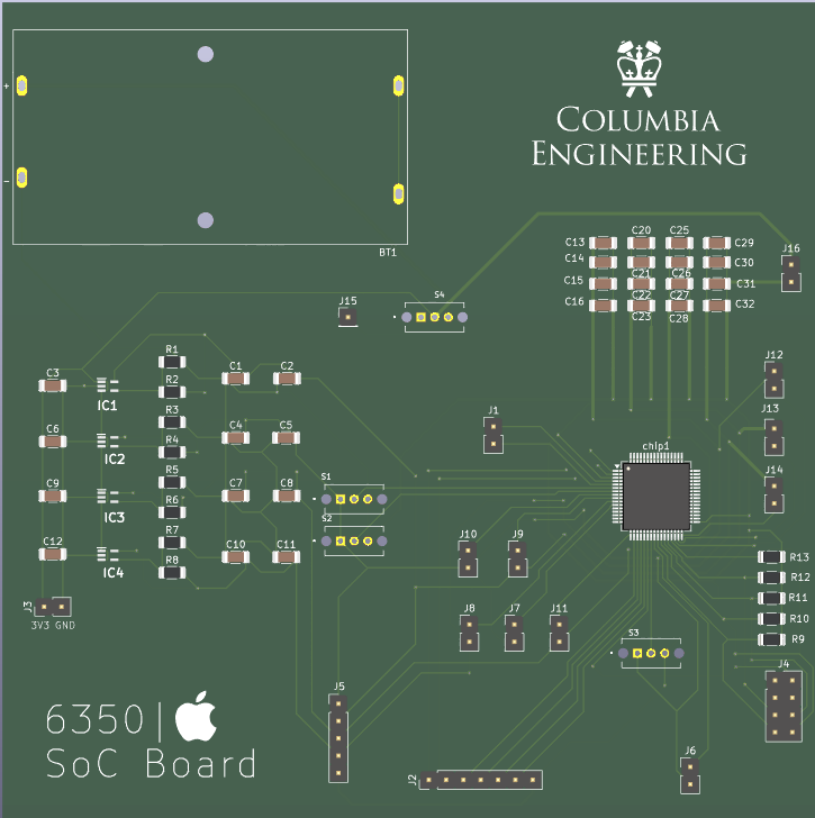
PCB Layout
Below shows the PCB Layout and PCB.
Demonstration
Demonstration Overview
We demonstrate a silicon-proven CPU–VPU heterogeneous RISC-V SoC on fabricated silicon.
The CPU orchestrates program control and system flow, while a custom Vector Processing Unit (VPU)
accelerates data-parallel kernels. This platform enables direct, reproducible comparisons between
scalar execution and vector offload under the same memory map, I/O path, and workload code structure.
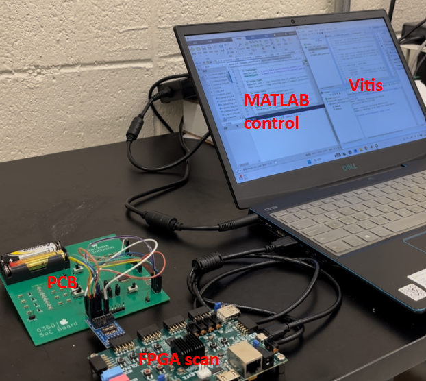
Demo Setup: PCB + FPGA Scan + MATLAB Control
The chip is mounted on a custom PCB and connected to an FPGA through a level shifter.
The FPGA handles low-level scan-in/scan-out pin toggling and basic control signals.
A MATLAB-based host script orchestrates the full loop: it streams the program and input data into on-chip memories,
triggers execution, then retrieves scan-out data to visualize outputs and compute performance metrics.
Each workload is executed in two modes using the same inputs, same memory map, and identical output locations:
- CPU-only: scalar inner loops on PicoRV32 (no vector offload).
- CPU+VPU: inner loops offloaded through custom PCPI vector instructions.
Speedup = Cycles(CPU-only) / Cycles(CPU+VPU).
Demo Flow
We prepared three workloads that cover high, medium, and low VPU utilization.
The goal is to show very clearly how VPU utilization translates into end-to-end speedup on our chip.
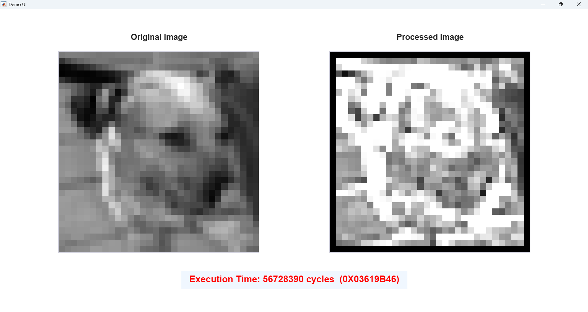
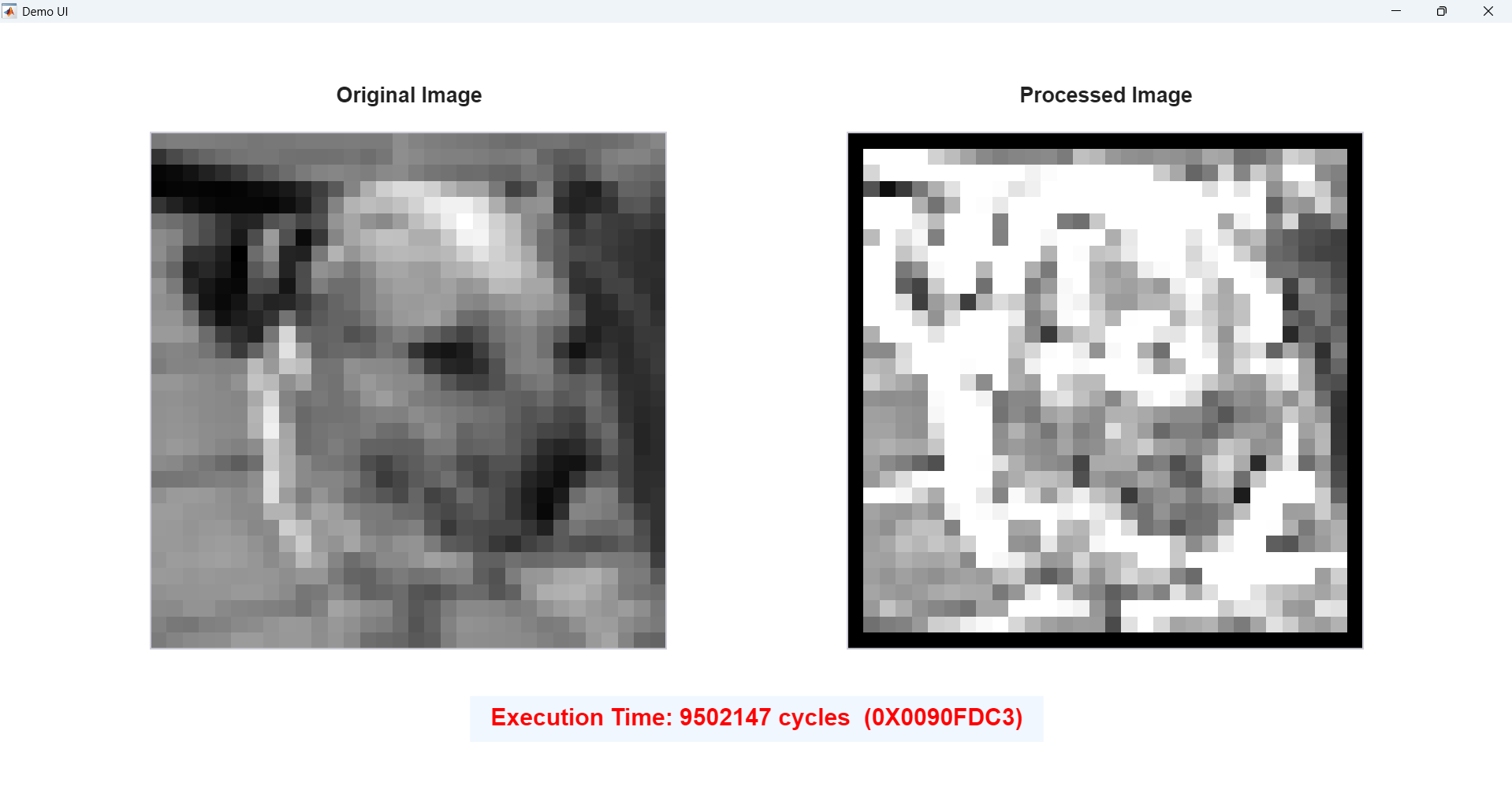
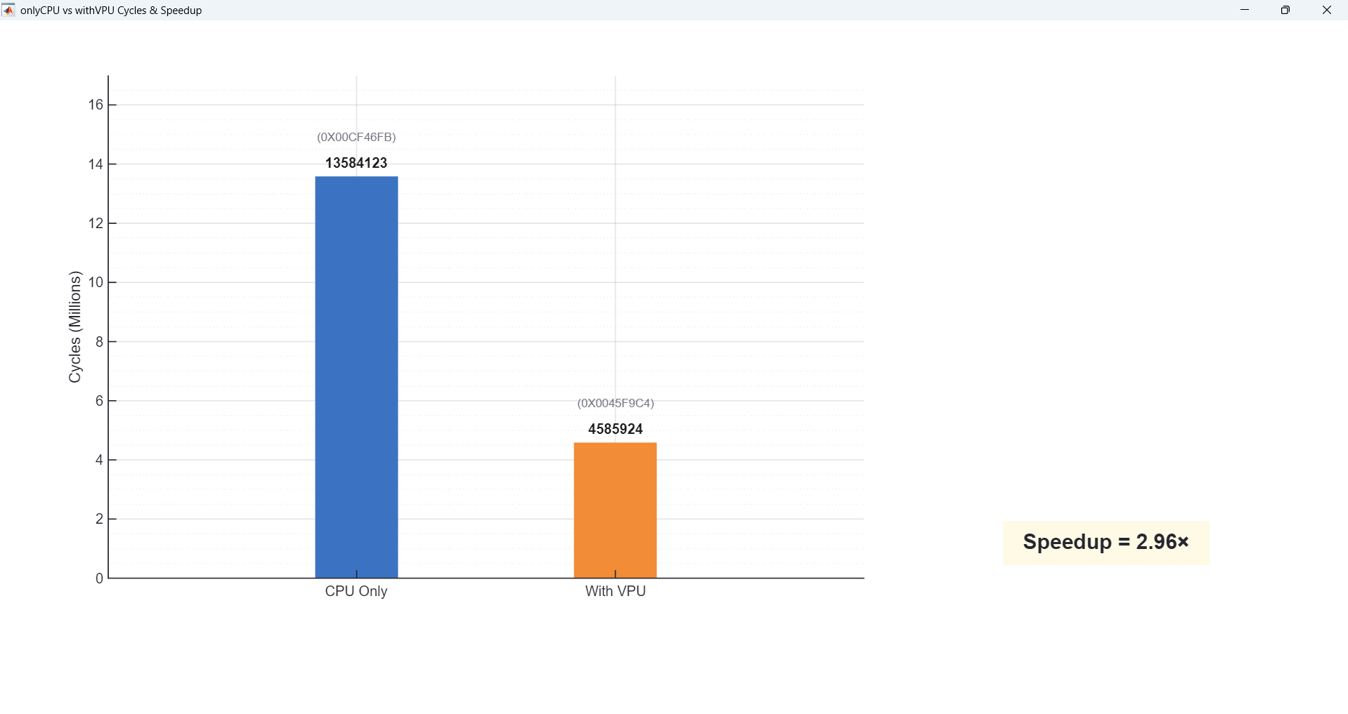
Demo 1 — CNN-style 4-Channel 3×3 Convolution
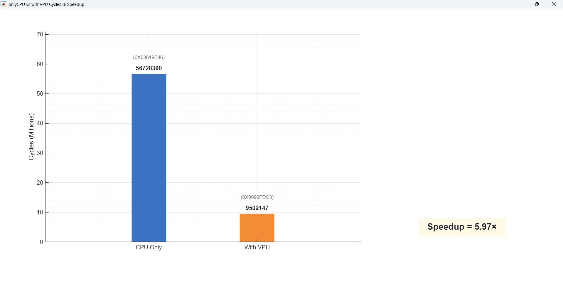
Demo 1 is a CNN-style 4-channel 3×3 convolution. Here almost every pixel goes through two 3×3 convolutions on four feature maps, so the code is very MAC-heavy. In this case, the VPU is active for around 80% of the total cycles, and we see a large speedup compared to the CPU-only baseline.
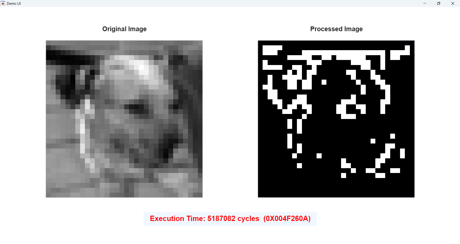
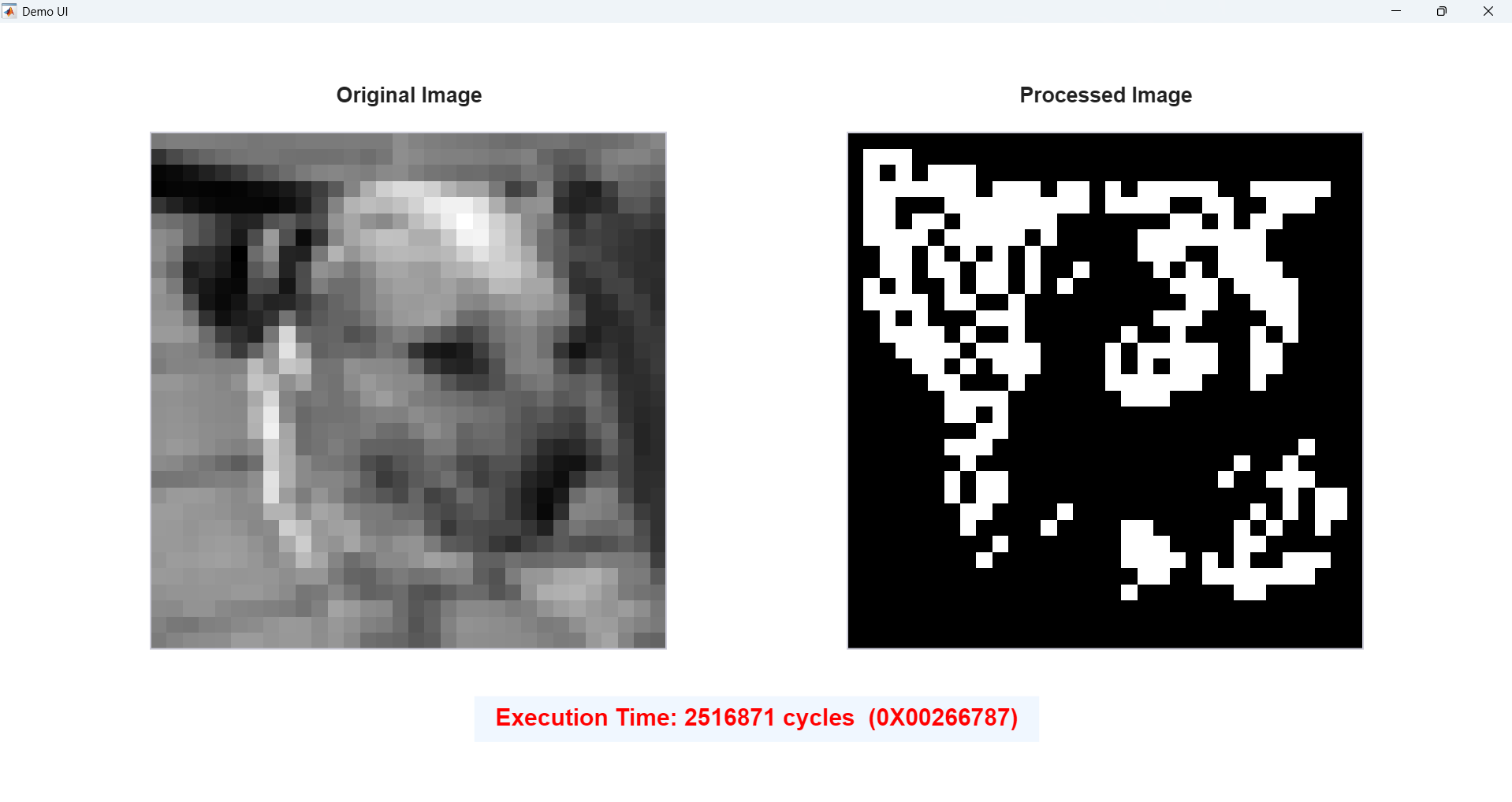
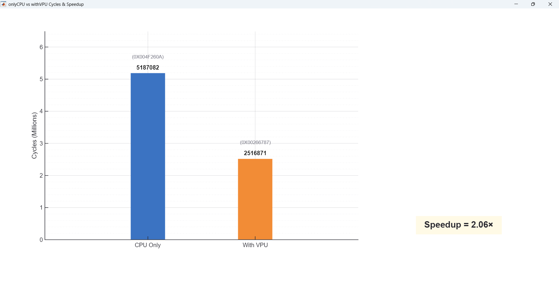
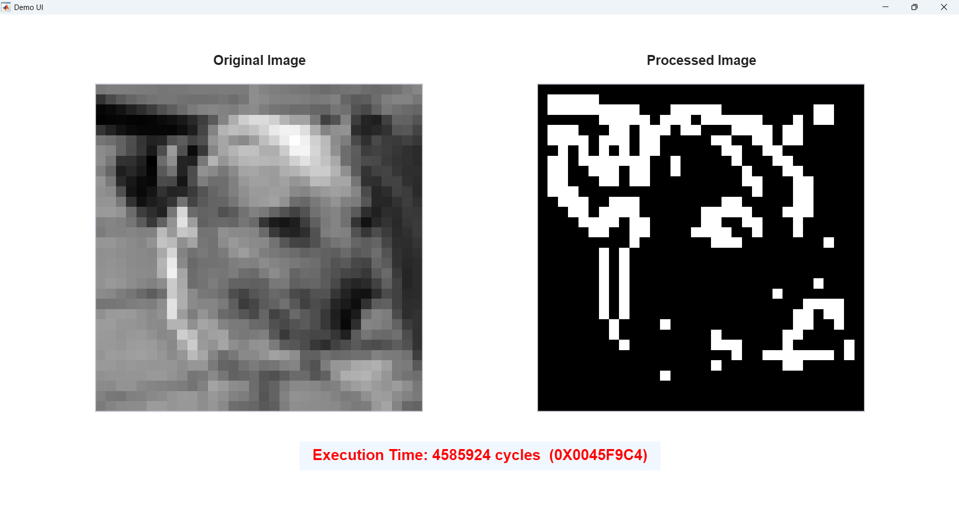
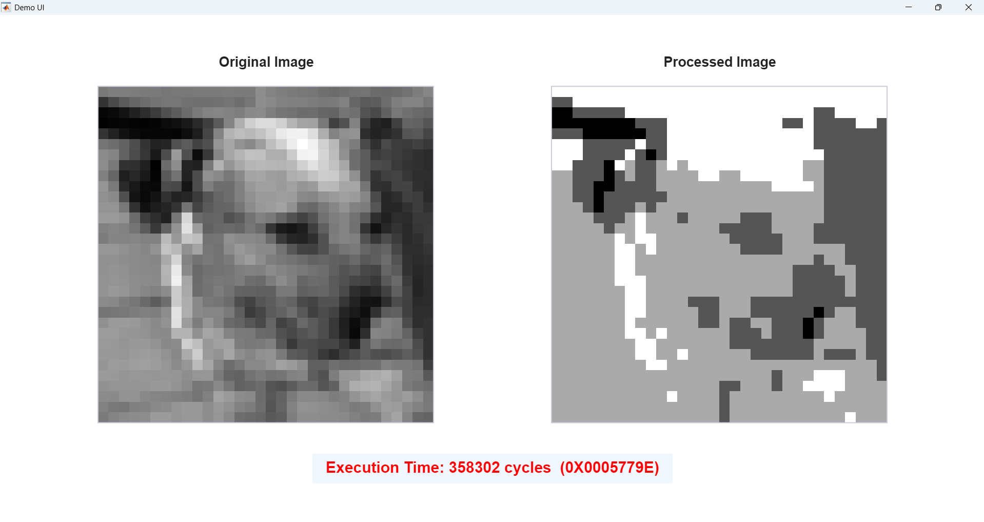
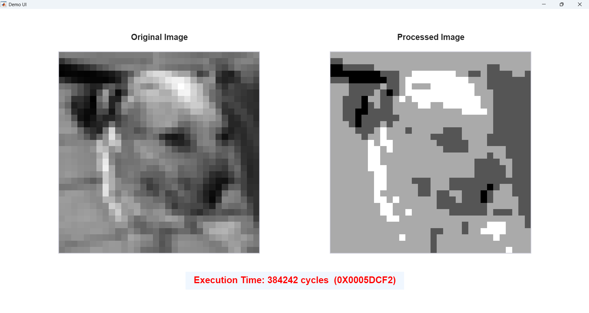
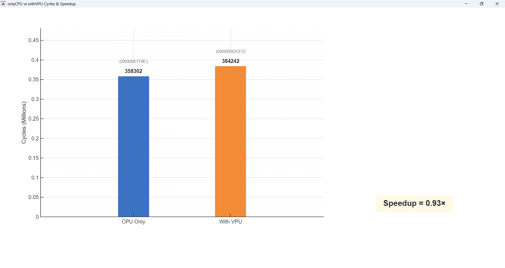
Demo 2 — Sobel Edge Detection (Full-frame vs. ROI-Sobel)
Demo 2 is edge detection with Sobel filters. We show two versions: full-frame Sobel, where we run VPU convolution on every pixel, and ROI-Sobel, where we first do a cheap scalar pre-check and only call the VPU on high-gradient regions. So full-frame Sobel uses the VPU for about 60% of the time, while ROI-Sobel is lower, around 45%. This demo highlights how even with the same algorithm family, changing the amount of VPU work shifts the speedup.

Demo 3 — 4-Level Posterize Filter
Demo 3 is a 4-level posterize filter. This is mostly simple per-pixel quantization with almost no vector multiply or convolution. Here the VPU utilization is only about 5%, and as a result we see very little acceleration — sometimes even slower — because the PCPI handshake + data movement cost dominates, and that overhead is larger than just doing the few adds/shifts directly on the CPU. As a result, end-to-end cycles are higher and the VPU appears “slower” for this posterize case.
So, across these three workloads, we sweep from VPU-heavy to light, and you can directly see how higher VPU utilization gives better speedup on our architecture.
Results Summary
Below summarizes our results. For the CNN-style 4-channel 3×3 convolution, the VPU is busy about 80% of the time (high utilization)
and we see roughly 6× speedup. For full-frame Sobel, VPU utilization drops to about 60% (medium utilization)
and the speedup is around 3×; with ROI Sobel, utilization is around 45% and the speedup is about 2×.
Finally, the 4-level posterize workload only uses the VPU about 5% of the time (low utilization), so the speedup is basically 1× — overhead dominates.
Overall, speedup clearly scales with vector intensity: the more time we spend in VPU-friendly vector math, the more benefit we get from our custom VPU.
This conclusion was also reached after processing a large amount of images and data.
| Workload | VPU Utilization | Speedup |
|---|---|---|
| CNN-style 4ch 3×3 Conv | ~80% (High) | ~6× |
| Sobel (Full-frame) | ~60% (Medium) | ~3× |
| Sobel (ROI) | ~45% (Medium–Low) | ~2× |
| Posterize (4-level) | ~5% (Low) | ~1× |
Video Demonstration
Chip Specifications
| Parameter | Specification |
|---|---|
| Technology | [TSMC 65nm LP] |
| Supporting ISAs | [RISCV32I and Custom Vector ISAs] |
| Memory(SRAM) | [32KB Data and 32KB Instruction] |
| Peripherals | [SPI and Uart] |
| Programming Interface | [Scan Chain] |
| Die Size | [2.0mm × 1.1mm] |
| Gate Count | [~766,000 gates] |
| Maxinum Operating Frequency | [252.52 MHz] |
| Supply Voltage | [1.0V core, 2.5V I/O] |
| Power Consumption | [13 mW typical] |
| Performance Metric | see in 'Demo' section |
| Package | [QFN-64] |
Internal Clock Frequency Table
| div[0:3] | fc[0:4] | Frequency (Hz) |
|---|---|---|
| 1111 | 11111 | 9.77k |
| 1111 | 01010 | 21.12k |
| 1111 | 00101 | 30.21k |
| 1110 | 01010 | 42.33k |
| 1110 | 00101 | 59.89k |
| 1101 | 01010 | 83.92k |
| 1101 | 00101 | 119.22k |
| 1100 | 01010 | 167.63k |
| 1100 | 00101 | 237.11k |
| 1011 | 01010 | 333.46k |
| 1011 | 00101 | 471.12k |
| 1010 | 01010 | 665.49k |
| 1010 | 00101 | 943.08k |
| 1001 | 01010 | 1.32M |
| 1001 | 00101 | 1.89M |
| 1000 | 01010 | 2.64M |
| 1000 | 00101 | 3.80M |
| 0111 | 01010 | 5.29M |
| 0111 | 00101 | 7.55M |
| 0110 | 01010 | 10.64M |
| 0110 | 00101 | 15.09M |
| 0101 | 01010 | 21.67M |
| 0101 | 00101 | 31.21M |
| 0100 | 01010 | 44.50M |
| 0100 | 00101 | 64.12M |
| 0011 | 01010 | 90.78M |
| 0011 | 00101 | 118.57M |
| 0010 | 01010 | 178.23M |
| 0010 | 00101 | 252.52M |
| 0001 | 01010 | 349.75M |
| 0001 | 00101 | 493.33M |
| 0000 | 01010 | 680.21M |
| 0000 | 00101 | 950.88M |
| 0000 | 00000 | 1.52G |
Conclusions
We taped out and demonstrated a silicon-proven CPU–VPU heterogeneous RISC-V SoC in TSMC 65 nm, featuring an in-house, custom-designed VPU attached to PicoRV32 via PCPI, along with on-chip IMEM/DMEM SRAM, essential I/O, and a scan-based bring-up/measurement flow. Live demos on fabricated silicon validate end-to-end hardware/software co-design and reveal a clear trend: end-to-end speedup increases monotonically with VPU utilization (vector intensity)—from ~1× on vector-light workloads to ~6× on convolution/MAC-heavy workloads. This behavior matches our architectural intent: the CPU orchestrates control flow while the VPU accelerates regular, data-parallel inner loops.
Key Achievements
- In-house custom VPU microarchitecture: Designed and implemented the VPU datapath and controller from scratch, including dedicated decode and multi-cycle control FSMs that manage instruction sequencing, base/stride address generation, memory handshaking, and PE scheduling—reducing CPU-side loop and address-update overhead.
- Custom Vector ISA + PCPI offload path: Created a custom vector ISA and integrated it through PicoRV32’s PCPI interface, enabling seamless CPU-issued vector offloads and clean, reproducible CPU-only vs. CPU+VPU benchmarking under the same workload structure and memory map.
- Silicon-proven SoC integration: PicoRV32 + custom VPU + on-chip IMEM/DMEM + peripherals were fully integrated and validated on fabricated silicon.
- Demo-ready post-silicon infrastructure: A repeatable MATLAB(PC) ⇄ FPGA(PMOD) ⇄ level shifter ⇄ PCB ⇄ chip pipeline supports scan-in / run / scan-out, automated visualization, and cycle-accurate performance measurement.
- Measured end-to-end scaling: CNN-style multi-channel convolution achieves the highest utilization and the largest speedup, while ROI-based and vector-light workloads show proportionally smaller gains as fixed offload and data-movement overhead becomes visible. As a result, our architecture is particularly well-suited for CNN-style AI kernels where computation is dominated by regular, vectorizable MAC patterns, making this SoC a compact AI-acceleration chip for convolution-heavy workloads.
Lessons Learned
- Acceleration is workload-dependent: The VPU delivers the biggest benefit when kernels are dominated by regular MAC/vector inner loops; when vector intensity is low, fixed PCPI and memory-transaction overhead can dominate and reduce (or negate) speedup.
- Co-design is essential: ISA design, memory layout, and measurement methodology must be aligned with the datapath and controller to obtain silicon-reproducible gains, not just isolated micro-benchmark wins.
- Bring-up infrastructure is first-class: A robust scan-based flow plus MATLAB/FPGA control significantly improves iteration speed and debugging confidence during post-silicon validation.
Future Work
- Reduce demo latency: Speed up scan-in/scan-out using higher scan clock, more efficient scan framing, or a higher-throughput debug interface to improve live-demo responsiveness.
- Scale beyond on-chip SRAM: Use SPI as a practical path to attach external storage (or an FPGA-based memory model) for larger tensors/weights and rapid re-parameterization of AI workloads.
- Increase VPU capability and observability: Extend the custom vector ISA (more ops, better reduction support, improved load/store patterns) and add lightweight performance counters to attribute cycles spent in CPU vs. VPU more precisely.
- Richer I/O demonstrations: Stream intermediate results and processed images more directly (e.g., UART-driven display pipeline) for more interactive, real-time demos.
References
- Clifford Wolf. PicoRV32 — A Size-Optimized RISC-V CPU. YosysHQ (GitHub repository). https://github.com/YosysHQ/picorv32
- Alex Forencich. verilog-axi — AXI and AXI-Stream Components for Verilog. (GitHub repository). https://github.com/alexforencich/verilog-axi
- Alex Forencich. verilog-axi: Tree / master (source code reference used for AXI modules/integration). https://github.com/alexforencich/verilog-axi/tree/master
- “pulp-platform/apb_spi_master,” GitHub, 2025. (accessed Dec. 15, 2025). https://github.com/pulp-platform/apb_spi_master
- AXI-4-Lite-to-APB3-Bridge, “GitHub - AXI-4-Lite-to-APB3-Bridge/AXI-4-Lite-to-APB3-Bridge,” GitHub, 2025. (accessed Dec. 08, 2025). https://github.com/AXI-4-Lite-to-APB3-Bridge/AXI-4-Lite-to-APB3-Bridge
- B. Green, D. Todd, J. C. Calhoun and M. C. Smith, "TIGRA: A Tightly Integrated Generic RISC-V Accelerator Interface," 2021 IEEE International Conference on Cluster Computing (CLUSTER), Portland, OR, USA, 2021, pp. 779-782, doi: 10.1109/Cluster48925.2021.00115.
- V. S. Chakravarthi and S. R. Koteshwar, SoC Physical Design. Springer Nature, 2022. verilog-axi: Tree / master (source code reference used for AXI modules/integration).
Acknowledgments
We want to sincerely thank everyone who supported us throughout this project and made our first tape-out and post-silicon bring-up possible.
First and foremost, we are deeply grateful to Prof. Mingoo Seok for his supervision and guidance throughout the project.
His technical expertise and hands-on feedback were invaluable at every stage, from architecture decisions to post-silicon validation.
Special thanks to our Teaching Assistants — Chuan-Tung Lin, Da Won Kim, and Mosom Jana — for their constant support.
They were always available to answer questions, troubleshoot issues, and help us overcome critical obstacles during design, integration, and bring-up.
We also thank Richard T. Lee for his help with the practical logistics of post-silicon testing, especially for supporting the purchase and preparation of the materials
needed for chip evaluation and measurement.
Finally, we gratefully acknowledge Apple Inc. for generous sponsorship and support. Without this sponsorship and the associated design review feedback,
this project would not have been possible.
Team Members
Back to all projects